
Product manual

CompactFlash Memory Card Product Manual Preliminary
SanDisk CompactFlash Memory Card Product Manual Rev. 8 © 2001 SANDISK CORPORATION
36
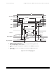
4.4 Card Configuration
The CompactFlash Memory Cards are identified
by appropriate information in the Card
Information Structure (CIS). The following
configuration registers are used to coordinate the
I/O spaces and the Interrupt level of cards that are
located in the system. In addition, these registers
provide a method for accessing status information
about the CompactFlash Card that may be used to
arbitrate between multiple interrupt sources on the
same interrupt level or to replace status
information that appears on dedicated pins in
memory cards that have alternate use in I/O cards.
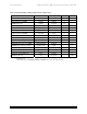
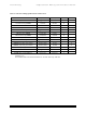
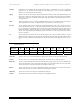
Table 4-11 Registers and Memory Space Decoding
-CE2 -CE1 -REG -OE -WE A10 A9 A8-A4 A3 A2 A1 A0 SELECTED SPACE
1 1 X X X X X XX X X X X Standby
X 0 0 0 1 X 1 XX X X X 0 Configuration Registers Read
1 0 1 0 1 X X XX X X X X Common Memory Read (8 Bit D7-D0)
0 1 1 0 1 X X XX X X X X Common Memory Read (8 Bit D15-D8)
0 0 1 0 1 X X XX X X X 0 Common Memory Read (16 Bit D15-D0)
X 0 0 1 0 X 1 XX X X X 0 Configuration Registers Write
1 0 1 1 0 X X XX X X X X Common Memory Write (8 Bit D7-D0)
0 1 1 1 0 X X XX X X X X Common Memory Write (8 Bit D15-D8)
0 0 1 1 0 X X XX X X X 0 Common Memory Write (16 Bit D15-D0)
X 0 0 0 1 0 0 XX X X X 0 Card Information Structure Read
1 0 0 1 0 0 0 XX X X X 0 Invalid Access (CIS Write)
1 0 0 0 1 X X XX X X X 1 Invalid Access (Odd Attribute Read)
1 0 0 1 0 X X XX X X X 1 Invalid Access (Odd Attribute Write)
0 1 0 0 1 X X XX X X X X Invalid Access (Odd Attribute Read)
0 1 0 1 0 X X XX X X X X Invalid Access (Odd Attribute Write)
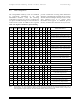
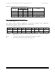
Configuration Registers Decoding
-CE2 -CE1 -REG -OE -WE A10 A9 A8-A4 A3 A2 A1 A0 SELECTED REGISTER
X 0 0 0 1 0 1 00 0 0 0 0 Configuration Option Reg Read
X 0 0 1 0 0 1 00 0 0 0 0 Configuration Option Reg Write
X 0 0 0 1 0 1 00 0 0 1 0 Card Status Register Read
X 0 0 1 0 0 1 00 0 0 1 0 Card Status Register Write
X 0 0 0 1 0 1 00 0 1 0 0 Pin Replacement Register Read
X 0 0 1 0 0 1 00 0 1 0 0 Pin Replacement Register Write
X 0 0 0 1 0 1 00 0 1 1 0 Socket and Copy Register Read
X 0 0 1 0 0 1 00 0 1 1 0 Socket and Copy Register Write
Note: The location of the card configuration registers should always be read from the CIS since these locations may vary in
future products. No writes should be performed to the CompactFlash Memory Card attribute memory except to the
card configuration register addresses. All other attribute memory locations are reserved.