
Product manual

Preliminary CompactFlash Memory Card Product Manual
SanDisk CompactFlash Memory Card Product Manual Rev. 8 © 2001 SANDISK CORPORATION
29
4.3.6.1 Common Memory Write Timing
The programming specification of various
memory devices are not standardized.
Moreover, programming specifications may
vary among different generations of the same
device. Consequently, it is not practical to set
standardized programming specifications for
these memory devices.
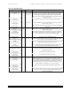
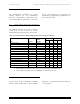
4.3.7 Attribute Memory Read Timing Specification
The Attribute Memory’s access time is defined
as 300 ns at 5 V Vcc or 600 ns at 3.3 Vcc.
Detailing timing specifications are shown below.
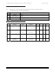
Table 4-5 Attribute Memory Read Timing Specification for all Types of Memory
300 ns 600 ns Speed Version
Item
Symbol
IEEE
Symbol
Min Min Max Max
Read Cycle Time t
c
R tAVAV 300 600
Address Access Time t
a
(A) tAVQV 300 600
Card Enable Access Time t
a
(CE) tELQV 300 600
Output Enable Access Time t
a
(OE) tGLQV 150 300
Output Disable Time from OE#
t
dis
(OE) tGHQZ 100 150
Output Enable Time from OE#
t
en
(OE) tGLQNZ 5 5
Data Valid from Add Change t
v
(A) tAXQX 0 0
Address Setup Time
1
t
su
(A) tAVGL 30 100
Address Hold Time
1
t
h
(A) tGHAX 20 35
Card Enable Setup Time
1
t
su
(CE) tELGL 0 0
Card Enable Hold Time
1
t
h
(CE) tGHEH 20 35
WAIT# Valid from OE#
1
t
v
(WT-OE) tGLWTV 35 100
WAIT# Pulse Width
2
T
w
(WT) tWTLWTH
12µs
12µs
Data Setup for WAIT# Released
2
t
v
(WT) tQVWTH 0 0
1. These timings are specified for hosts and PC Cards which support the WAIT# signal.
2. These timings are specified only when WAIT# is asserted within the cycle.
4.3.8 Attribute Memory Write Timing Specification
In the absence of other information, Attribute
Memory Write timing shall be 250 ns SRAM
timing for 5 V operation and 600 ns timing for
3.3 V operation.