
User Manual


SanDisk CompactFlash Card OEM Product Manual Interface Description
02/09, Rev. 1.0 ii © 2007 - 2009 SanDisk Corporation. SanDisk Confidential, subject to all applicable non-disclosure agreements.
12
3 Interface Description
3.1 Physical Description
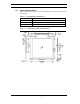
The host connects to SanDisk CompactFlash Memory cards using a standard 50-pin connector
consisting of two rows of 25 female contacts each on 50 mil (1.27 mm) centers.
3.1.1 Pin Assignments and Types
The signal/pin assignments are listed in Table 3-1. Low active signals have a "-" prefix. Pin
types are Input, Output or Input/Output. Sections 3.3.1 and 3.3.2 define the DC characteristics
for all input and output type structures..
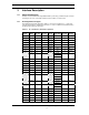
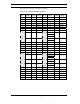
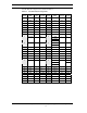
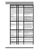
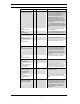
Table 3-1 PC Card Memory Mode Pin Assignments
Pin No.
Signal
Name Pin Type I/O Type Pin No. Signal Name Pin Type I/O Type
1 GND Ground 26 -CD1 O Ground
2 D03 I/O I1Z, OZ3 27 D11 I/O I1Z, OZ3
3 D04 I/O I1Z, OZ3 28 D12 I/O I1Z, OZ3
4 D05 I/O I1Z, OZ3 29 D13 I/O I1Z, OZ3
5 D06 I/O I1Z, OZ3 30 D14 I/O I1Z, OZ3
6 D07 I/O I1Z, OZ3 31 D15 I/O I1Z, OZ3
7 -CE1 I I3U 32 -CE2 I I3U
8 A10 I I1Z 33 -VS1 O Ground
-IORD
HSTROBE
9 -OE I I3U 34
-HDMARDY
I I3U
10 A09 I I1Z 35 -IOWR I I3U
11 A08 I I1Z 36 -WE I I3U
12 A07 I I1Z 37 READY O OT1
13 VCC Power 38 VCC Power
14 A06 I I1Z 39 -CSEL I I2Z
15 A05 I I1Z 40 -VS2 O OPEN
16 A04 I I1Z 41 RESET I I2Z
-WAIT
-DDMARDY
10
17 A03 I I1Z 42
DSTROBE
11
O OT1
-INPACK 18 A02 I I1Z 43
-DMARQ
12
O OT1
-REG 19 A01 I I1Z 44
-DMACK
12
I I3U
20 A00 I I1Z 45 BVD2 O OT1
21 D00 I/O I1Z, OZ3 46 BVD1 O OT1
22 D01 I/O I1Z, OZ3 47 D08
1
I/O I1Z, OZ3
23 D02 I/O I1Z, OZ3 48 D09
1
I/O I1Z, OZ3
24 WP O OT3 49 D10
1
I/O I1Z, OZ3
25 -CD2 O Ground 50 GND Ground