SanDisk CompactFlash Memory Card OEM Product Manual Version 3.0 Document No. 20-10-00038 March 2010 SanDisk Corporation Corporate Headquarters 601 McCarthy Boulevard Milpitas, CA 95035 (408) 801-1000 Phone (408) 801-8657 Fax www.sandisk.com 03/09, Rev. 1.0 ii © 2007 - 2009 SanDisk Corporation. SanDisk Confidential, subject to all applicable non-disclosure agreements.
SanDisk CompactFlash Card OEM Product Manual SanDisk® Corporation general policy does not recommend the use of its products in life support applications wherein a failure or malfunction of the product may directly threaten life or injury.
SanDisk CompactFlash Card OEM Product Manual Table of Contents Table of Contents 1 Introduction.......................................................................................................................... 4 1.1 1.2 1.3 1.4 1.5 1.6 1.7 2 Product Specifications ......................................................................................................... 8 2.1 2.2 2.3 2.4 3 General Description.......................................................................................
SanDisk CompactFlash Card OEM Product Manual 1 Introduction 1.1 General Description Introduction SanDisk CompactFlash® Memory Card products provide high capacity solid-state flash memory that electrically complies with the Personal Computer Memory Card International Association ATA (PC Card ATA) standard. (In Japan, the applicable standards group is JEIDA.) The CompactFlash Memory Card Series also supports a True IDE Mode that is electrically compatible with an IDE disk drive.
SanDisk CompactFlash Card OEM Product Manual 1.2 Introduction Features SanDisk CompactFlash Memory cards provide the following system features: • • • • • • • • • • • • • 1.3 Up to 64 GB of mass storage data PC Card ATA protocol compatible True IDE Mode compatible Very low CMOS power Very high performance Very rugged Low weight Noiseless Low Profile +3.3 Volts operation +5.
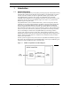
SanDisk CompactFlash Card OEM Product Manual Introduction Documentation can be ordered from IHS by calling 1-800-854-7179 or accessing their Web site: http://global.ihs.com. 1.7 Functional Description CompactFlash Memory cards contain a high level, intelligent subsystem as shown in the block diagram, Figure 1-1. This intelligent (microprocessor) subsystem provides many capabilities not found in other types of memory cards.
SanDisk CompactFlash Card OEM Product Manual 1.7.5 Introduction Automatic Sleep Mode A unique feature of the SanDisk CompactFlash Memory Card is automatic entrance and exit from sleep mode. Upon completion of a command, the card will enter sleep mode to conserve power if no further commands are received within 5 msec. The host does not have to take any action for this to occur. In most systems, the CompactFlash Memory Card is in sleep mode except when the host is accessing it, thus conserving power.
SanDisk CompactFlash Card OEM Product Manual 2 Product Specifications Product Specifications For all the following specifications, values are defined at ambient temperature and nominal supply voltage unless otherwise stated. 2.1 System Environmental Specifications Table 2-1 contains environmental specifications which include temperature, humidity, acoustic noise, vibration, shock and altitude.
SanDisk CompactFlash Card OEM Product Manual a Memory Subsystem Product Specifications CompactFlash 400x Memory Card Sleep 1 mA 1.2 mA Read 500 mA 500 mA Write 500 mA 500 mA Read/ Write Peak 500 mA 500 mA a. Maximum Average Value. 02/09, Rev. 1.0 ii © 2007 - 2009 SanDisk Corporation. SanDisk Confidential, subject to all applicable non-disclosure agreements.
SanDisk CompactFlash Card OEM Product Manual 2.3 Product Specifications System Performance All performance timings assume the CompactFlash Memory Card Series controller is in the default (i.e., fastest) mode. Table 2-3 Performance CompactFlash 85x Memory Card Start-up Times Sleep to Write 2.5 ms maximum Sleep to Read 20 ms maximum Reset to Ready 120 ms typical; 400 ms maximum 25.
SanDisk CompactFlash Card OEM Product Manual 2.4 Product Specifications Physical Specifications Refer to Table 2-5 and see Figure 2-1 for CompactFlash Memory Card physical specifications and dimensions. Table 2-5 CompactFlash Physical Dimensions Weight 11.4 g (.40 oz) typical, 14.2 g (.50 oz) maximum Length 36.40 ± 0.15 mm (1.433 ± .006 in) Width 42.80 ± 0.10 mm (1.685 ± .004 in) Thickness 3.3 mm ± 0.10 mm (.130 ± .
SanDisk CompactFlash Card OEM Product Manual 3 3.1 Interface Description Interface Description Physical Description The host connects to SanDisk CompactFlash Memory cards using a standard 50-pin connector consisting of two rows of 25 female contacts each on 50 mil (1.27 mm) centers. 3.1.1 Pin Assignments and Types The signal/pin assignments are listed in Table 3-1. Low active signals have a "-" prefix. Pin types are Input, Output or Input/Output. Sections 3.3.1 and 3.3.
SanDisk CompactFlash Card OEM Product Manual Interface Description PC Card I/O Pin Assignments are contained in Table 3-2. Table 3-2 PC Card I/O Mode Pin Assignments Pin No. Signal Name 1 GND 2 D03 3 4 Pin Type Pin No.
SanDisk CompactFlash Card OEM Product Manual Interface Description True IDE Mode Pin Assigments are contained in Table 3-3. Table 3-3 True IDE Mode Pin Assignments Pin No. Signal Name Pin Type Pin No.
SanDisk CompactFlash Card OEM Product Manual 3.2 Interface Description Electrical Description The CompactFlash Memory Card Series is optimized for operation with hosts, which support the PCMCIA I/O interface standard conforming to the PC Card ATA specification. However, the card may also be configured to operate in systems that support only the memory interface standard.
SanDisk CompactFlash Card OEM Product Manual Signal Name Interface Description Dir. Pin -CD1, -CD2 (True IDE Mode) -CE1, -CE2 (PC Card Memory Mode) Card Enable Description This signal is the same for all modes. I 7,32 These input signals are used both to select the card and to indicate to the card whether a byte or a word operation is being performed. -CE2 always accesses the odd byte of the word. -CE1 accesses the even byte or the Odd byte of the word depending on A0 and -CE2.
SanDisk CompactFlash Card OEM Product Manual Signal Name Interface Description Dir. Pin -INPACK (PC Card I/O Mode except Ultra DMA Protocol Active) Input Acknowledge Description The Input Acknowledge signal is asserted by the CompactFlash Storage Card or CF+ Card when the card is selected and responding to an I/O read cycle at the address that is on the address bus.
SanDisk CompactFlash Card OEM Product Manual Signal Name Interface Description Dir. Pin Description -HDMARDY (All Modes - Ultra DMA Protocol DMA Read) In all modes when Ultra DMA mode DMA Read is active, this signal is asserted by the host to indicate that the host is ready to receive Ultra DMA data-in bursts. The host may negate –HDMARDY to pause an Ultra DMA transfer.
SanDisk CompactFlash Card OEM Product Manual Signal Name READY (PC Card Memory Mode) Interface Description Dir. O Pin 37 Description In Memory Mode, this signal is set high when the CompactFlash Storage Card or CF+ Card is ready to accept a new data transfer operation and is held low when the card is busy. At power up and at Reset, the READY signal is held low (busy) until the CompactFlash Storage Card or CF+ Card has completed its power up or reset function.
SanDisk CompactFlash Card OEM Product Manual Signal Name RESET (PC Card Memory Mode) Interface Description Dir. I Pin 41 Description The CompactFlash Storage Card or CF+ Card is Reset when the RESET pin is high with the following important exception: The host may leave the RESET pin open or keep it continually high from the application of power without causing a continuous Reset of the card. Under either of these conditions, the card shall emerge from power-up having completed an initial Reset.
SanDisk CompactFlash Card OEM Product Manual Signal Name Interface Description Dir. Pin DSTROBE (All Modes – Ultra DMA Read Protocol Active) -WE (PC Card Memory Mode) Description In all modes, when Ultra DMA mode DMA Read is active, this signal is the data in strobe generated by the device. Both the rising and falling edge of DSTROBE cause data to be latched by the host. The device may stop generating DSTROBE edges to pause an Ultra DMA data in burst.
SanDisk CompactFlash Card OEM Product Manual 3.3 Interface Description Electrical Specification All D.C. Characteristics for the CompactFlash Memory Card Series are defined as follows: Typical conditions unless otherwise stated: VCC = 5V +/- 10% Tolerant VCC = 3.3V +/- 5% Ta = 0° C to 60° C Absolute Maximum Conditions: VCC = -0.3V min. to 6.5V max. V* = 0.5V min. to VCC + 0.5V max. *Voltage on any pin except VCC with respect to GND. 3.3.
SanDisk CompactFlash Card OEM Product Manual Interface Description Table 3-6 defines the input characteristics of the parameters in Table 3-5. Table 3-6 Input Characteristics Min. Type 1 2 3 Parameter Symbol Max. Min. VCC=3.3V Input Voltage CMOS Vih Vil 2.0 Input Voltage CMOS Vih Vil 2.0 Input Voltage CMOS Schmitt Trigger Typ. Typ. Max. 2.0 Volts 0.8 0.8 2.0 Volts 0.8 1 Vt+(Vp) 2 Vt-(Vn) 3 Vh(ΔVt) Unit VCC=5.0V 0.9 0.7 0.2 2.1 1.9 1.4 0.8 0.9 0.7 0.2 2.1 1.9 1.
SanDisk CompactFlash Card OEM Product Manual 2 Output Voltage 3 X Output Voltage Tri-State Leakage Current Interface Description Voh Ioh = -4 mA Vol Iol = 4 mA Voh Ioh = -4 mA Vol Iol = 4 mA Ioz Vol = Gnd Voh = Vcc Volts 2.4V 0.4V 2.4V Volts 0.4V -10 10 µA In UDMA modes greater than 4, the characteristics specified in the following table apply. Voltage output high and low values shall be met at the source connector to include the effect of series termination.
SanDisk CompactFlash Card OEM Product Manual 4 ATA Command Set ATA Command Set The following table defines the complete list of commands supported by the CompactFlash card. Specifics of each command’s operation can be found in the CF+ & CF SPECIFICATION REV. 4.1.
SanDisk CompactFlash Card OEM Product Manual 5 Identify Device–ECH Identify Device–ECH The following table defines the specifics of the Identify Data returned by the CompactFlash card. Specifics of each word can be found in the CF+ & CF SPECIFICATION REV. 4.1. Table 5-8 Identify Device Information Word Address Default Value Total Bytes 0 848Ah 2 General configuration bit-significant information 0XXX 2 General configuration – Bit Significant with ATA-4 definitions.
SanDisk CompactFlash Card OEM Product Manual Table 5-8 Identify Device–ECH Identify Device Information Word Address Default Value Total Bytes 51 0200h 2 PIO data transfer cycle timing mode 52 0000h 2 Single word DMA data transfer cycle timing mode (not supported) Data Field Type Information 53 0003h 2 Field validity 54 XXXXh 2 Current number of cylinders 55 XXXXh 2 Current number of heads 56 XXXXh 2 Current sectors per track 57-58 XXXXh 4 Current capacity in sectors (LBAs)
SanDisk CompactFlash Card OEM Product Manual Table 5-8 Identify Device–ECH Identify Device Information Word Address Default Value Total Bytes 163 XXXXh 2 CF Advanced True IDE Timing Mode Capability and Setting 164 XXXXh 2 CF Advanced PCMCIA I/O and Memory Timing Mode Capability 165-175 0000h 22 Reserved for assignment by the CFA 176-255 0000h 140 Reserved Data Field Type Information a. Multiword DMA is supported by SanDisk PCMCIA.
SanDisk CompactFlash Card OEM Product Manual 6 CIS Description CIS Description This section describes the Card Information Structure (CIS) for SanDisk CompactFlash Memory cards.
SanDisk CompactFlash Card OEM Product Manual Table 6-1 CIS Description Card Information Structure Attribute Offset Data 026h 00h 7 6 5 4 3 2 1 High Byte of PCMCIA Manufacturer’s Code 0 Content Description CIS Function Code of 0 because other byte is JEDEC 1 byte Manufacturer’s ID High Byte of PCMCIA Low Byte Product Code Mfg ID 028h 01h Low Byte of Product Code SanDisk Code for SDP Series 02Ah 04h High Byte of Product Code SanDisk Code for PC Card ATA High Byte Product Code 0
SanDisk CompactFlash Card OEM Product Manual Table 6-1 CIS Description Card Information Structure Attribute Offset Data 7 6 5 4 3 2 1 0 062h 14h W 12 NI PP P D RIA RIR SP 0 0 1 1 1 0 0 N A 0 Content Description CIS Function No Wear Level & NO Vpp SanDisk Fields, 1 to 4 W: No Wear Level 12: Vpp not used on Write NI: -INPACK connected PP: Programmable Power Bytes limited by link length PDNA: Pwr Down Not Abort--Cmd RIA: RBsy, ATBsy connected RIR: RBsy Inhibited at Reset S
SanDisk CompactFlash Card OEM Product Manual Table 6-1 CIS Description Card Information Structure Attribute Offset Data 074h 01h Disk Function Extension Tuple Type 076h 01h Interface Type Code 078h 22h CISTPL_FUNCE 7 6 5 4 3 2 1 0 Content Description CIS Function Extension Tuple describes the Interface Extension Tuple Type Protocol 07Ah 03h 07Ch 02h PC Card–ATA Interface Function Extension tuple Tuple has 3 Info Bytes Disk Function Extension Tuple Type for Disk Extension In
SanDisk CompactFlash Card OEM Product Manual Table 6-1 CIS Description Card Information Structure Attribute Offset Data 086h 01h 7 6 5 4 3 2 1 RFS RMS RAS 00 00 01 0 Content Description CIS Function Size of Reserved Field Size of Fields Byte (TPCC_SZ) is 0 Bytes Size of Register Mask is 1 Byte Size of Config Base Address is 2 Bytes RFS: Bytes in Reserved Field RMS: Bytes in Reg Mask–1 RAS: Bytes in Base Addr–1 088h 08Ah 08Ch 08Eh 0Fh 07h TPCC_LAST 00h TPCC_RADR (LSB) 02h TP
SanDisk CompactFlash Card OEM Product Manual Table 6-1 CIS Description Card Information Structure Attribute Offset Data 7 6 5 4 096h C0h W R P B 1 1 0 0 3 2 1 0 Interface Type Content Description CIS Function Memory Only Interface(0), Bvd's and wProt not used, TPCE_IF Ready/-Busy and Wait for memory cycles active.
SanDisk CompactFlash Card OEM Product Manual Table 6-1 CIS Description Card Information Structure Attribute Offset Data 7 6 5 4 3 0A8h 21h X R P RO A T 0 0 1 0 0 1 2 1 0 Content Description CIS Function Power-Down and Twin Card.
SanDisk CompactFlash Card OEM Product Manual Table 6-1 CIS Description Card Information Structure Attribute Offset Data 0BEh C1h 7 6 5 4 3 2 1 I D Configuration Index 1 1 1 0 Content Description CIS Function I/O Mapped Contiguous 16 Registers Configuration. Configuration Index for this entry is 1. Interface Byte follows this byte. TPCE_INDX Default Configuration, therefore is not 0C0h 41h W 0 R 1 P 0 B 0 dependent on previous Default Configuration.
SanDisk CompactFlash Card OEM Product Manual Table 6-1 CIS Description Card Information Structure Attribute Offset Data 7 0C8h 4Dh X 0 9h = 4.5 5h = 1V X Mantissa Exponent 0 Bh = 5.5 5h = 1V X Mantissa Exponent 0CAh 0CCh 5Dh 75h 6 64h R 0 4 3 2 Mantissa 0 0CEh 5 0 Exponent Eh = 8.0 S 1 1 E 1 Content Description CIS Function VCC Nominal is 4.5V VCC Min. Value VCC Nominal is 5.5V VCC Max. Max. Average Current Max.
SanDisk CompactFlash Card OEM Product Manual Table 6-1 CIS Description Card Information Structure Attribute Offset Data 7 6 5 4 3 0D6h 21h X R P RO A T 0 0 1 0 0 1 2 1 0 Content Description Power-Down and Twin Card. CIS Function TPCE_MI T: Twin Cards Allowed A: Audio Supported RO: Read Only Mode P: Power Down Supported R: Reserved X: More Misc Fields Bytes 0D8h 1Bh 0DAh 06h CISTPL_CE Configuration Entry Tuple Link to Next Tuple is 6 Bytes.
SanDisk CompactFlash Card OEM Product Manual Table 6-1 CIS Description Card Information Structure Attribute Offset Data 7 6 5 4 0EEh 41h W R P B 0 1 0 0 3 2 1 0 Interface Type 1 Content Description CIS Function I/O Interface(1), Bvd's and wProt not used; Ready/-Busy active but Wait not used for memory cycles .
SanDisk CompactFlash Card OEM Product Manual Table 6-1 CIS Description Card Information Structure Attribute Offset Data 7 6 5 0FCH EAh R S E 1 1 1 0FEh 61h LS 1 Content Description CIS Function IO AddeLines Ah = 10 Supports both 8- and 16-bit I/O hosts. 10 Address Lines with range so card will respond only to indicated (1F0-1F7, 3F6-3F7) on A9 through A0 for I/O cycles.
SanDisk CompactFlash Card OEM Product Manual Table 6-1 CIS Description Card Information Structure Attribute Offset Data 7 6 5 4 10Ch EEh S P L M0 1 1 1 3 2 1 0 Recommend IRQ Level Eh = 14 Content Description CIS Function IRQ Sharing Logic Active in Card Control & Status Register, Pulse and Level Mode Interrupts supported, Recommended IRQ's TPCE_IR any of 0 through 15(F) S: Share Logic Active P: Pulse Mode IRQ Supported L: Level Mode IRQ Supported M: Bit Mask of IRQs Present M=0 s
SanDisk CompactFlash Card OEM Product Manual Table 6-1 CIS Description Card Information Structure Attribute Offset Data 7 11Ch 1Eh X 0 11Eh 4Dh X Mantissa 0 9h = 4.5 120h 1Bh 122h 12h 6 5 4 3 Content Description CIS Function +.30 Nominal Operation Supply Voltage Extension Exponent Max. Average Current Max. Average 5h = 10 over 10 ms is 45 mA Current Configuration Entry Tuple Tuple Code Link to Next Tuple is 18 Bytes. Also limits size of this tuple to 20 bytes.
SanDisk CompactFlash Card OEM Product Manual Table 6-1 CIS Description Card Information Structure Attribute Offset Data 7 6 5 4 3 2 1 0 12Ah 27h R DI PI AI SI HV LV NV 0 0 1 0 0 1 1 1 Content Description Nominal Voltage Follows NV: Nominal Voltage LV: Mimimum Voltage CIS Function Power Parameters for VCC HB: Maximum Voltage SI: Static Current AI: Average Current PI: Peak Current DI: Power Down Current 12Ch 12Eh 130h 55h 4Dh 5Dh X Mantissa Exponent 0 Ah = 5.
SanDisk CompactFlash Card OEM Product Manual Table 6-1 CIS Description Card Information Structure Attribute Offset Data 136h 61h 7 6 5 4 3 2 1 LS AS N Ranges–1 1 2 1 0 Content Description Number of Ranges is 2; Size of each address is 2 bytes; size of each length is 1 byte.
SanDisk CompactFlash Card OEM Product Manual Table 6-1 CIS Description Card Information Structure Attribute Offset Data 7 6 5 4 3 146h 21h X 0 R0 P 1 RO 0 A0 2 1 0 T Content Description Power-Down, and Twin Card. 1 CIS Function TPCE_MI T: Twin Cards Allowed A: Audio Supported RO: Read Only Mode P: Power Down Supported R: Reserved X: More Misc Fields Bytes 148h 1Bh 14Ah 06h 14Ch 03h CISTPL_CE Configuration Entry Tuple Tuple Code Link to Next Tuple is 6 Link to Bytes.
SanDisk CompactFlash Card OEM Product Manual Table 6-1 CIS Description Card Information Structure Attribute Offset Data Content Description CIS Function 164h 014h CISTPL_NO_LINK Prevent scan of common memory Tuple Code 166h 000h No Bytes following Link Length is 0 Bytes Link to Next Tuple 168h 0FFh End of Tuple Chain End of CIS Tuple Code 7 6 5 4 3 2 1 0 a. Legacy CompactFlash products may report “SunDisk” as the ASCII manufacture string 02/09, Rev. 1.
SanDisk CompactFlash Memory Card Appendix: Ordering Information Appendix: Ordering Information A1. SanDisk CompactFlash Memory Card1 SanDisk products directly from SanDisk, call (408) 801-1000. Capacity Part Number No. of (formatted in Sectors/Card bytes) Sectors/ (Max. LBA+1) No. of Heads Tracks No.