
User Manual


CompactFlash Memory Card Interface Description
3-8 CompactFlash
®
Memory Card Product Manual, Rev. 10.0 © 2002 SANDISK CORPORATION
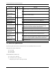
3.3.4. Output Drive Characteristics
Table 3-6. Output Drive Characteristics
Type Parameter Symbol Conditions MIN TYP MAX Units
1 Output Voltage Voh
Vol
Ioh = -4 mA
Iol = 4 mA
Vcc
-0.8V
Gnd
+0.4V
Volts
2 Output Voltage Voh
Vol
Ioh = -8 mA
Iol = 8 mA
Vcc
-0.8V
Gnd
+0.4V
Volts
3 Output Voltage Voh
Vol
Ioh = -8 mA
Iol = 8 mA
Vcc
-0.8V
Gnd
+0.4V
Volts
X Tri-State
Leakage Current
Ioz Vol = Gnd
Voh = Vcc
-10 10 µA
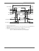
3.3.5. Common Memory Read Timing
Table 3-7. Common Memory Read Timing Specification for all Types of Memory
100 ns Speed Version tem Symbol IEEE Symbol
Min Max
Read Cycle Time t
c
(R) tAVAV 100
Address Access Time
1
t
a
(A) tAVQV 100
Card Enable Access Time t
a
(CE) tELQV 100
Output Enable Access Time t
a
(OE) tGLQV 50
Output Disable Time from -OE t
dis
(OE) tGHQZ 50
Output Disable Time from -CE t
dis
(CE) tEHQZ 50
Output Enable Time from -CE t
en
(CE) tELQNZ 5
Output Enable Time from -OE t
en
(OE) tGLQNZ 5
Data Valid from Add Change
1
t
v
(A) tAXQX 0
Address Setup Time t
su
(A) tAVGL 10
Address Hold Time t
h
(A) tGHAX 15
Card Enable Setup Time t
su
(CE) tELGL 0
Card Enable Hold Time t
h
(CE) tGHEH 15
1. The -REG signal timing is identical to address signal timing.
2. SanDisk CompactFlash Memory Cards do not assert the -WAIT Signal.
NOTE: All timings measured at the CompactFlash Memory Card. Skews and delays from the system
driver/receiver to the CompactFlash Memory Card must be accounted for by the system.