
User's Manual


page 17/64
Note d’étude / Technical document : URD1– OTL
5665.3
– 003 / 72238 Edition 01
Document Sagemcom Reproduction et divulgation interdites
Sagemcom document. Reproduction and disclosure prohibited
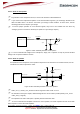
4.4 NETWORK LED
The HiLoNC V2 module can manage a network LED. The LED can be connected either to one of the available
GPIO or to a PWM (but not the one dedicated to the buzzer).
The transistors can be found a in a single package referenced as UMDXX or PUMDXX Family.
Value of resistor R depends on characteristic of chosen LED; it is used to limit the current through the diode.
Use the AT command to set the GPIO or PWM used to control the LED.
Figure 12: Network LED connection
4.5 POWER SUPPLY
The HiLoNC V2 module can be supplied by a battery or any DC/DC converter compliant with the module supply
range 3.2V to 4.5V and 2.2 A.
The PCB tracks must be well dimensioned to support 2.2 A maximum current (Burst current 1.8A plus the
extra current for the other used I/Os). The voltage ripple caused by serial resistance of power supply path
(Battery internal resistance, tracks and contact resistance) could result in the voltage drops.
To prevent any issue in the power up procedure the typical rise time for VBAT should be 1ms.
The HiLoNC V2 module does not manage the battery charging.
4.5.1 Burst conditions
- Communication mode (worst case: 2 continuous GSM time-slot pulse):
Figure 13: GSM/GPRS Burst Current rush
A 47µF with Low ESR capacitor is highly recommended for VBAT and close to the module pads 30 & 31.
GPIO or
PWM
HiLoNC V2
VBAT
R