
Technical information


Procedure
Proc 0 01
Proc 1 01
Proc 1 02
Proc 1 03
Proc 1 04
Proc 1 05
Proc 1 08
Proc 1 10
Proc 1 18
Proc 1 20
Proc 1 22
Proc 2 01
Proc 2 03
Proc 3 01
Proc 3 02
Proc 4 01
Symptom
Symp 01
Symp 02
Symp 03
Symp 04
Symp 05
Symp 06
Symp 07
Symp 08
Symp 10
Test
Test 01
Test 02
Test 03
Test 04
Test 05
Test 06
Proc Sheet 4 01
myC3-2
5HPRYHDQG3ODFHWKH,2FRQQHFWRU
3/3
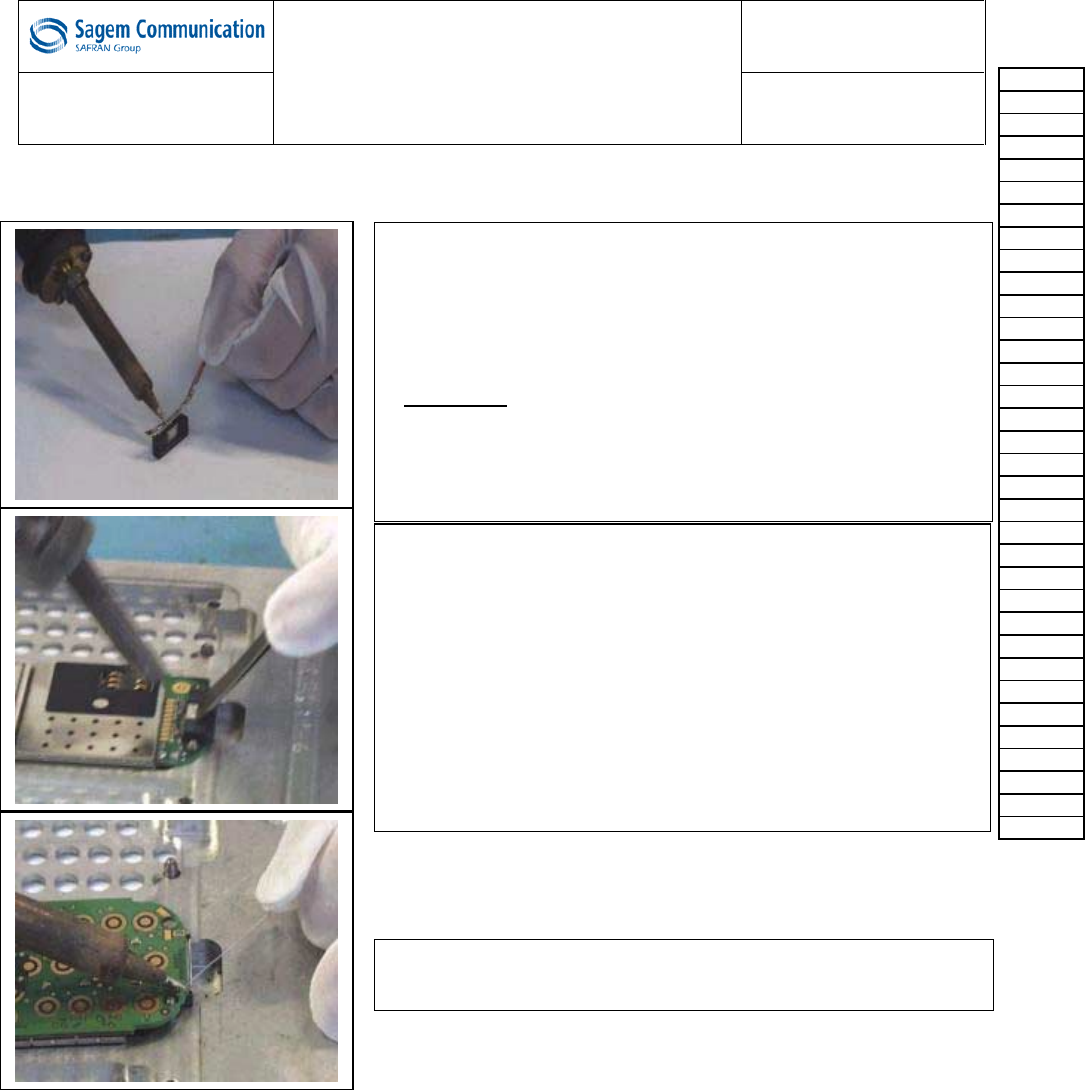
Before any operation,
-flux correctly the pins of the connector.
-with the solder wick loaded with tin , tin the pins of the
DATA/ AUDIO/ CHARGE connector by positioning it
straight ahead (pads upward), and by heating the solder
wick which is in touch with pins.
$WWHQWLRQ
- At the end of the operation , verify that there is no short
circuit between pads.
Start soldering the connector pins.
-Flux the place of the connector and position the DATA/
AUDIO/ CHARGE connector.
-Verify that the pins of the DATA/ AUDIO/ CHARGE
connector are well centred on pads.
-Heat pins with an air blow device while maintaining the
connector with tweezers
9HULI\WKDWWKHUHLVQRVKRUWFLUFXLWWKDWVROGHUVDUH
VKLQ\DQGWKDWWKH\FRYHUZHOOWKHSLQV
At last, solder the 4 pins crossing the board..
Contents REF MTB DTS 1- Indice D - November 10 2005 Page 5-34