
Instruction Manual

Réf. : SCT TMO MASV3 SPEC
30
Rev. : H
Réf. sec. : 2x xxx xxx – x
Date : 12/05/04
DRAFT
Document
. All rights of reproduction and disclosure reserved.
Page 20
This document contains information on a product under development. SAGEM reserves the right to change or discontinue this product
without notice.
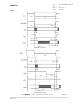
Single access:
7LPLQJ
'HVFULSWLRQ
0LQQV
0D[QV
t
cyc
CPU frequency
-
1/F
cpu
t
csv
Chip Select Valid
t
cyc
(N+1)t
cyc
t
da
NCS to Address valid
-
1.2
t
ha
Address hold from nCS
0
-
t
dbe
NBHE, nBLE to nCS
-
0.6
t
doe
NOE to nCS
-
0.6
t
su
Input data setup to nCS
5.5
-
t
ho
Input data hold from nCS
0
-
t
srw
NCS to RnW
T
cyc
/2-t
drw
-
t
drw
RnW to nCS
1.3
2.9
t
dso
NCS to output data valid
-
T
srw
+7.5
t
hd
Output data hold from RnW
0
-
N= Wait State number
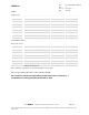
Page mode access:
7LPLQJ
'HVFULSWLRQ
0LQQV
0D[QV
t
cyc
CPU frequency
-
1/F
cpu
t
csv
Chip Select Valid
t
cyc
(N+1)t
cyc
t
da
NCS to Address valid
-
1.5
t
ha
Address hold from nCS
0
-
t
dbe
NBHE, nBLE to nCS
-
0.8
t
doe
NOE to nCS
-
1.5
t
su1
Input data setup to nCS
5.2
-
t
ho1
Input data hold from nCS
0
-
t
su2
Input data setup to nCS
5.6
-
t
ho2
Address invalid time
-
3
T
sa1sa2
Input data hold from nCS
0
-
Note: all timings computed for an external capacitance load of 10pF
NB: if needed, additional Wait State could be added by SAGEM.
%HFDUHIXOWKHPD[LPXPFDSDFLWDQFHFRPSRQHQWVOLQHVFRQQHFWRUV«
DFFHSWDEOHRQHDFKVLJQDORIWKHSDUDOOHOEXVLVS)