
Installation Instruction
Ref : SCT TMO MOD SPEC 662
Rev.: B
Ref. sec. :
Date:
18/11/2004
Document
%
. All rights of reproduction and disclosure reserved.
MO2XX module – Confidential under NDA
Page 34/67
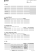
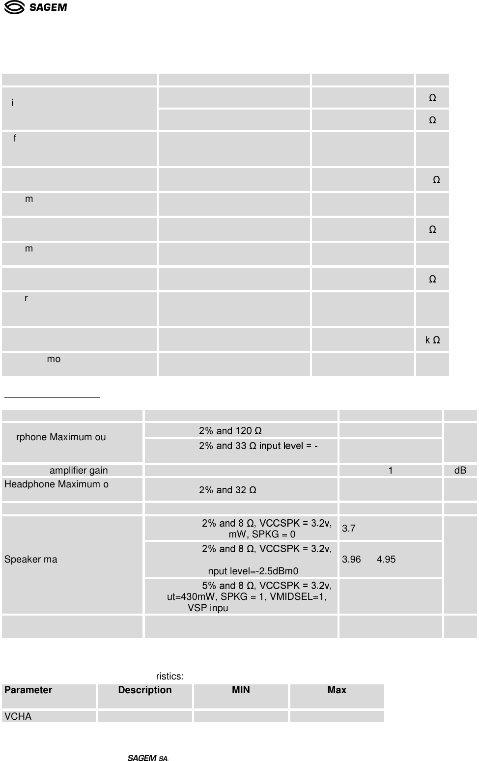
Parameter Tests Conditions
Min Typ Max
Units
Output swing 3.9 Vpp 120
&
Differential Minimum resistive load
between HPP32 and HPN32 ; R//
Output swing 1.5 Vpp 33
&
Differential Maximum capacitor
load between HPP32 and HPN32;
C//
100
pF
Common mode Minimum resistive
load at HPP32 and HPN32
200 k
&
Common mode Maximum load at
HPP32 and HPN32
10
pF
Minimum resistive load at HSOL
and HSOR: R//
32
&
Maximum capacitor load at HSOL
and HSOR: C//
100
pF
Differential Minimum resistive load
between HPP8 and HPN8: R//
Output swing 4.38 Vpp 8
&
Differential Maximum capacitor
load between HPP8 and HPN8:
C//
100
pF
Common mode Minimum resistive
load at HPP8 and HPN8
200
')(
Common mode Maximum
capacitor load at HPP8 and HPN8
10
pF
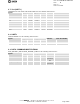
Global Characteristics
Parameter Tests Conditions
Min Typ Max
Units
Distortion
≤
*,+.-0/21435*7698
3.1 3.92
Earphone Maximum output
swing at HPP32 - HPN32
Distortion
≤
:,;.<0=2>@?7?9A B CEDEF$GIH JLKMJ0HONQP
5.34dBm0
1.2 1.5
Vpp
Earphone amplifier gain 1 dB
Headphone Maximum output
swing at (HSOL/R)
Distortion
≤
R,S.T0C2U@VLRXW
1.6 1.96 Vpp
Headphone L/R amplifier gain -5 dB
Distortion
≤
Y,Z.[0\2]@^Q_ `badcdcfehgjilkXm0n oqpE`
Pout=340mW, SPKG = 0
3.73 4.66
Distortion
≤
o,r.s0t2u@vQwx`badcdcfehgjilkXm0n oqpE`
Pout=380mW, SPKG = 1, VMIDSEL=1,
VSP input level=-2.5dBm0
3.96 4.95Speaker maximum output at
HPP8 - HPN8
Distortion
≤
yEz.{0|2}@~QxbddfhjlX0 qE
Pout=430mW, SPKG = 1, VMIDSEL=1,
VSP input level=-2dBm0
4.2 5.24
Vpp
Speaker amplifier gain
SPKG=0
SPKG=1
2.5
8.5
dB
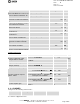
6.12 CHARGER
Charger has the following characteristics:
Parameter Description MIN Max
VCHARGEUR Charger voltage 6V 7V
See details on Application Note