
Datasheet


Technical Note
3/17
LM358DT/PT/ST/WDT/WPT,LM2904DT/PT/ST/WDT/WPT
LM324DT/PT/WDT,LM2902DT/PT/WDT
www.rohm.com
2011.06 - Rev.B
© 2011 ROHM Co., Ltd. All rights reserved.
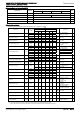
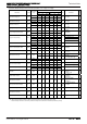
○LM2904,LM2902 family(Unless otherwise specified, Vcc+=+5[V], Vcc-=0[V])
Parameter Symbol
Temperature
range
Limit
Unit Conditions
Fig.
No
LM2904 family LM2902 family
Min. Typ. Max. Min. Typ. Max.
Input Offset Voltage (*3) VIO
25℃ - 2 7 - 2 7
mV VO=1.4[V] 98
Full range - - 9 - - 9
Input Offset Current (*3) IIO
25℃ - 2 50 - 2 30
nA VO=1.4[V] 98
Full range - - 200 - - 200
Input Bias Current (*3) IIB
25℃ - 20 150 - 20 150
nA VO=1.4[V] 98
Full range - - 200 - - 300
Large Signal Voltage Gain AVD 25℃ 25 100 - 25 100 - V/mV
Vcc
+
=15[V]
VO=1.4[V] to 11.4[V]
RL=2[kΩ]
98
Supply Voltage Rejection Ratio SVR
25℃ 65 100 - 65 110 -
dB RS≦10[kΩ] 99
Full range 65 - - 65 - -
Supply Current (All Amp) ICC
25℃ - 0.7 1.2 - 0.7 1.2
mA
Vcc
+
=5[V],No Lord
99
25℃ - - - - 1.5 3 Vcc
+
=30[V],No Lord
Full range - - 2 - 0.8 1.2 Vcc
+
=5[V],No Lord
Full range - - - - 1.5 3 Vcc
+
=30[V],No Lord
Input Common-mode Voltage Range VICM
25℃ - - Vcc
+
-1.5 - - Vcc
+
-1.5
V Vcc
+
=30[V] 98
Full range - - Vcc
+
-2.0 - - Vcc
+
-2.0
Common-mode Rejection Ratio CMR
25℃ 70 85 - 70 80 -
dB RS=10[kΩ] 98
Full range 60 - - 60 - -
Output Short Circuit Current (*4) Isource 25℃ 20 40 60 20 40 70 mA
Vcc
+
=+15[V],VO=+2[V]
VID=+1[V]
98
Output Sink Current (*4) Isink 25℃
10 20 - 10 20 - mA
VO=2[V],Vcc
+
=+5[V]
VID=-1[V]
99
12 50 - 12 50 - μA
VO=+0.2[V],
Vcc
+
=+15[V] ,VID=-1[V]
Output Voltage Swing Vopp
25℃ 0 - Vcc
+
-1.5 - - -
V RL=2[kΩ] 99
Full range 0 - Vcc
+
-2.0 - - -
High Level Output Voltage VOH
25℃ 27 - - 27 28 -
V
Vcc
+
=30[V],RL=10[kΩ]
99
Full range 27 28 - 27 - - Vcc
+
=30[V],RL=10[kΩ]
Low Level Output Voltage
VOL
25℃ - 5 20 - 5 20
mV RL=10[kΩ] 99
Full range - - 20 - - 20
Slew Rate SR 25℃ - 0.6 - - 0.4 - V/μs
RL=2[kΩ],CL=100[pF],
Unity Gain
VI=0.5[V] to 3[V]
Vcc
+
=1.5[V]
99
Gain Bandwidth Product GBP 25℃ - 1.1 - - 1.3 - MHz
Vcc
+
=30[V],RL=2[kΩ]
CL=100[pF]
VIN=10[mV]
99
Total Harmonic Distortion THD 25℃ - 0.02 - - 0.015 - %
f=1[kHz],AV=20[dB]
RL=2[kΩ]
CL=100[pF],
Vcc
+
=30[V],VO=2[Vpp]
99
Input Equivalent Noise Voltage en 25℃ - - - - 40 -
HznV/
f=1[kHz],RS=100[Ω]
Vcc
+
=30[V]
99
Input Offset Voltage Drift DVIO - - 7 - - 7 - μV/℃ - -
Input Offset Current Drift DIIO - - 10 - - 10 - pA/℃ - -
Channel Separation VO1/VO2 25℃ - 120 - - 120 - dB 1[kHz]≦f≦20[kHz] 99
(*3) Absolute value
(*4) Under high temperatures, please consider the power dissipation when selecting the output current.
When the output terminal is continuously shorted the output current reduces the internal temperature by flushing.