
Datasheet


Technical Note
12/17
LM358DT/PT/ST/WDT/WPT,LM2904DT/PT/ST/WDT/WPT
LM324DT/PT/WDT,LM2902DT/PT/WDT
www.rohm.com
2011.06 - Rev.B
© 2011 ROHM Co., Ltd. All rights reserved.
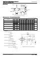
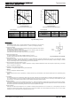
●Circuit Diagram
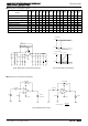
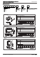
●Measurement Circuit 1 NULL Method Measurement Condition
Vcc
+
, Vcc
-
, EK, Vicm Unit: [V]
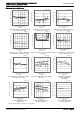
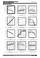
Parameter VF S1 S2 S3
LM358/LM324 family LM2904/LM2902 family
Calculation
Vcc+ Vcc- EK Vicm Vcc+ Vcc- EK Vicm
Input Offset Voltage VF1 ON ON OFF 5 to 30 0 -1.4 0 5 to 30 0 -1.4 0 1
Input Offset Current VF2 OFF OFF OFF 5 0 -1.4 0 5 0 -1.4 0 2
Input Bias Current
VF3 OFF ON
OFF
5 0 -1.4 0 5 0 -1.4 0
3
VF4 ON OFF 5 0 -1.4 0 5 0 -1.4 0
Large Signal Voltage Gain
VF5
ON ON ON
15 0 -1.4 0 15 0 -1.4 0
4
VF6 15 0 -11.4 0 15 0 -11.4 0
Common-mode Rejection Ratio
VF7
ON ON OFF
5 0 -1.4 0 5 0 -1.4 0
5
VF8 5 0 -1.4 3.5 5 0 -1.4 3.5
Supply Voltage Rejection Ratio
VF9
ON ON OFF
5 0 -1.4 0 5 0 -1.4 0
6
VF10 30 0 -1.4 0 30 0 -1.4 0
-Calculation-
1. Input Offset Voltage (VIO)
2. Input Offset Current (IIO)
3. Input Bias Current (IIB)
4. Large Signal Voltage Gain (AVD)
5.Common-mode Rejection Ration (CMRR)
6. Supply Voltage Rejection Ration (SVR)
Fig.98 Measurement circuit1 (Each Op-Amps)
Fig.97 Circuit Diagram (each Op-Amp)
OUTPUT
INVERTING
INPUT
NON-INVERTING
INPUT
Vcc
+
Vcc
-
△
Vcc
+
=25V
PSRR
=
20×Log
△
Vcc
+
×(1+Rf/Rs)
VF10 - VF9
[dB]
VF8-VF7
Rs)Rf
/
(1+
Log
CMRR
3.5×
[dB]
20×
VF6 - VF5
/Rs)R
f
(1+
Log20×
10×
AV
[dB]
Rf / Rs)
(1+ Ri2×
VF3
VF4 -
Ib
[A]
/ Rs)R
f
(1+Ri
VF1VF2 -
Iio
[A]
[V]
/RsR
f
1+
VF1
Vio
50[Ω]
50[Ω]
10[kΩ]
10[kΩ]
50[kΩ]
50[kΩ]
500[kΩ]
500[kΩ]
VOUT
R
f
EK
S1
S2
S3
Ri
Ri
Rs
Rs
R
f
RL
Vicm
DUT
Vcc
+
Vcc
-
VF
0.1[μF]
0.1[μF]
1000[pF]
+15[V]
-15[V]
V