
Datasheet

SEMICONDUCTOR LSI BU9438KV 4/4
A TSZ02201-BU9438KV-1-2
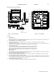
◇External dimensions・Block diagram
10.0±0.1
12.0±0.2
10.0±0.1
12.0±0.2
0.5±0.15
0.145
1 16
17
32
33
48
49
64
1.6MAX
1.4±0.05
0.1±0.05
0.2
0.5±0.1
1 PIN mark1.25
1.25
+0.05
-0.04
0.08 S
4゜
+6゜
-4゜
+0.05
-0.03
1.0±0.2
BU9438KV
Lot No.
0.08
M
( UNIT : mm )
1 2 3 4 5 6 7 8 9 10 11 12 13 14 15 16
55
54
53
52
51
50
49
23
22
21
20
19
18
17
39 38 37 36 35 34 33
24
28
27
26
25
31
30
29
32
43 42 41 4047 46 45 4448
59
58
57
56
61
60
63
62
64
AMUTE
DAVDD
RESETX
SEL_SLAVE
SEL_MP3
SEL_DOUT
SEL_VOL
SEL_APLAY
SEL_UTPKT
TEST1
KEY_ROW1/
MCHNG
KEY_ROW2/
BUSY
KEY_COL1/A0
DVDDIO
TEST3
SD_CON
TMODE
DVSS
LED_PUSB/TEST12
LED_PSD/TEST11
LED_PLAY/TEST10
DAVSS
LED_ACCESS
LED_ERROR/TEST9
XOUT_PLL
XIN_PLL
TEST_PLL
REXTI
AVSSC
SD_CLK
SD_DI
SD_CS
DVSS
TEST4
TEST5/
CLKOUT12
DVDD_M2
TEST6
TEST7
AVDDC
TEST2
SD_DO
TEST8
VOREFI
VDDPLL
LED_RANDOM
TEST17
TEST16
TEST15
LED_REPEAT
DVDDIO
ATEST1
RDACO
VCDACO
Audio DAC
AAC / WMA /
MP3
Decoder
PLL
USB
PHY
System
Controller
FAT
File system
KEY_ROW4/SDA
TEST13
DVDD_M1
TEST14
SD I/F
Controller
Sound Effecter
KEY_ROW3/SCL
KEY_COL2/A1
KEY_COL3/
SEL_SMAN
USB_DM
USB_DP
VSS_PLL
LDACO
USB
Controller
LDO
I2C I/F
Controller
Figure 1. External dimention Figure 2. Block diagram
◇
Caution
(1) Power on Reset
Please keep the termina
l RESETX at the Low level when the power supply starts. After completely starting up 3.3V system power supply , afterwards,
please make the terminal RESETX High level after 5us after the oscillation of the system clock is steady. Moreover, please make the
terminal RESETX
Low level during 5us or more when resetting it while operating..
(2) About compatibility in USB memory device and SD memory card
According to the file structure and communication speed of an USB memory, SD memory card, this LSI might not play back correctly.
(3) About turning on the power supply
Current rush might flow momentarily by the order of turning on the power supply and the delay in IC with two or more power supplies, and note the
capacity of the power supply coupling, the power supply, and width and drawing the GND pattern wiring.
(4) About absolute maximum rating
When the absolute maximum rating such as the applied voltage and the ranges of the operating temperature
is exceeded, LSI might be destroyed. Please apply neither voltage nor the temperature that exceeds the
absolute maximum rating. Please execute physical measures for safety such as fuse when it is thought to
exceed the absolute maximum rating, and examine it so that the condition to exceed the absolute maximum
rating is not applied to LSI.
(5) About GND Voltage
In any state of operation must be the lowest voltage about the voltage of the terminal GND. Please actually confirm the voltage of each terminal is not a
voltage that is lower than the terminal GND including excessive phenomenon.
(6) About design of overheating malfunction preventive circuit
Please design overheating malfunction preventive circuit with an enough margin in consideration of a permissible loss in the state of using actually.
(7) About the short between terminals and the mounting by mistake
Please note the direction and the gap of position of LSI enough about LSI when you mount on the substrate. LSI might be destroyed when mounting by
mistake and energizing. Moreover, LSI might be destroyed when short-circuited by entering
of the foreign substances between the terminal and GND,
between terminals, between the terminal and the power supply of LSI.
(8) About operation in strong electromagnetic field
Use in strong electromagnetic field has the possibility of malfunctioning and evaluate it enough, please.
PKG: VQFP64
Drawing No. EX252-5001-1