
Datasheet


15/16
BR25L010-W, BR25L020-W, BR25L040-W, BR25L080-W, BR25L160-W, BR25L320-W, BR25L640-W
Technical Note
Notes on power ON/OFF
Noise countermeasures
POR circuit
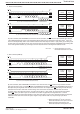
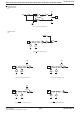
Fig.63 CS timing at power ON/OFF
Bad example
Good example
GND
Vcc
GND
Vcc
Vcc
CS
At power ON/OFF, set CS "H" (= VCC).
When CS is "L", this IC gets in input accept status (active). If power is turned on in this status, noises and the likes may cause
malfunction, mistake write or so. To prevent these, at power ON, set CS "H". (When CS is in "H" status, all inputs are canceled.)
(Good example) CS terminal is pulled up to V
CC.
At power OFF, take 10ms or higher before re supply. If power is turned on without observing this condition, the IC internal
circuit may not be reset, which please note.
(Bad example) CS terminal is "L" at power ON/OFF.
In this case, CS always becomes "L" (active status), and EEPROM may have malfunction, mistake write owing to noises
and the likes.
Even when CS input is High-Z, the status becomes like this case, which please note.
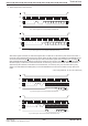
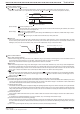
This IC has a POR (Power On Reset) circuit as mistake write countermeasure. After POR action, it gets in write disable status. The POR
circuit is valid only when power is ON, and does not work when power is OFF. When power is ON, if the recommended conditions of the
following tR, tOFF, and Vbot are not satisfied, it may become write enable status owing to noises and the likes.
Vcc noise (bypass capacitor)
When noise or surge gets in the power source line, malfunction may occur, therefore, for removing these, it is recommended to attach a
by pass capacitor (0.1µF) between IC Vcc and GND. At that moment, attach it as close to IC as possible.
And, it is also recommended to attach a bypass capacitor between board Vcc and GND.
SCK noise
When the rise time (tR) of SCK is long, and a certain degree or more of noise exists, malfunction may occur owing to clock bit displacement.
To avoid this, a Schmitt trigger circuit is built in SCK input. The hysteresis width of this circuit is set about 0.2V, if noises exist at SCK input,
set the noise amplitude 0.2Vp-p or below. And it is recommended to set the rise time (tR) of SCK 100ns or below. In the case when the rise
time is 100ns or higher, take sufficient noise countermeasures. Make the clock rise, fall time as small as possible.
WP noise
During execution of write status register command, if there exist noises on WP pin, mistake in recognition may occur and forcible cancellation
may result, which please note. To avoid this, a Schmitt trigger circuit is built in WP input. In the same manner, a Schmitt trigger circuit is
built in SI input and HOLD input too.
Cautions on use
(1) Described numeric values and data are design representative values, and the values are not guaranteed.
(2) We believe that application circuit examples are recommendable, however, in actual use, confirm characteristics further sufficiently. In the case
of use by changing the fixed number of external parts, make your decision with sufficient margin in consideration of static characteristics
and transition characteristics and fluctuations of external parts and our LSI.
(3) Absolute maximum ratings
If the absolute maximum ratings such as impressed voltage and operating temperature range and so forth are exceeded, LSI may be destructed.
Do not impress voltage and temperature exceeding the absolute maximum ratings. In the case of fear exceeding the absolute maximum
ratings, take physical safety countermeasures such as fuses, and see to it that conditions exceeding the absolute maximum ratings should
not be impressed to LSI.
(4) GND electric potential
Set the voltage of GND terminal lowest at any action condition. Make sure that each terminal voltage is lower than that of GND terminal.
(5) Heat design
In consideration of permissible dissipation in actual use condition, carry out heat design with sufficient margin.
(6) Terminal to terminal short circuit and wrong packaging
When to package LSI onto a board, pay sufficient attention to LSI direction and displacement. Wrong packaging may destruct LSI. And in
the case of short circuit between LSI terminals and terminals and power source, terminal and GND owing to foreign matter, LSI may be
destructed.
(7) Use in a strong electromagnetic field may cause malfunction, therefore, evaluate design sufficiently.
Recommended conditions of tR, tOFF, Vbot
10ms or below
tR tOFF Vbot
100ms or below
0.3V or below
0.2V or below
10ms or higher
10ms or higher
Fig.64Pgqcu_tcdmpk
tR
tOFF
Vbot
V
CC
0
2010.07 -
Rev. B
www.rohm.com
© 2010 ROHM Co., Ltd. All rights reserved.