
Datasheet

9/16
BR25L010-W, BR25L020-W, BR25L040-W, BR25L080-W, BR25L160-W, BR25L320-W, BR25L640-W
Technical Note
Write status register command can write status register data. The data the can be written by this command are 2 bits *1,
that is, BP1 (bit3) and BP0 (bit2) among 8 bits of status register. By BP1 and BP0, write disable block of EEPROM can be
set. As for this command, set CS LOW, and input ope code of write status register, and input data. Then, by making CS
HIGH, EEPROM starts writing. Write time requires time of tE/W as same as write. As for CS rise, start CS after taking the
last data bit (bit0), and before the next SCK clock starts. At other timing, command is cancelled. Write disable block is
determined by BP1 and BP0, and the block can be selected from 1/4 of memory array, 1/2, and entire memory array.
(Refer to the write disable block setting table.) To the write disabled block, write cannot be made, and only read can be
made.
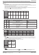
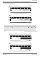
Fig.41 Status register write command (BR25L010/020/040-W)
0
00 00 0
* 0 1 BP1 BP0
bit0bit1bit2bit3bit4bit5bit6bit7
123456789101112131415
CS
SCK
SI
SO
High
-
Z
**** **
* =
Don't care
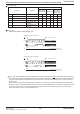
Fig.42 Status register write command (BR25L080/160/320/640-W)
0
00 0 0 0 001 BP1BP0
bit0bit1bit2bit3bit4bit5bit6bit7
123456789101112131415
CS
SCK
SI
SO
High
-
Z
*** * *
WPEN
* =
Don't care
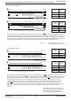
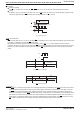
Fig.43 Status register read command (BR25L010/020/040-W)
0
00 00 011
123456 789101112131415
CS
SCK
SI
SO
High
-
Z
bit0bit1bit2bit3bit4bit5bit6bit7
BP11111 BP0
WEN
R/B
*
* =
Don't care
Fig.44 Status register read command (BR25L080/160/320/640-W)
00 000 011
High
-
Z
bit0bit1bit2bit3bit4bit5bit6bit7
BP1 BP0
WEN
WPEN
000
R/B
SI
SO
0 1 2 3 4 5 6 7 8 9 10 11 12 13 14 15
CS
SCK
4. Status register write / read command
* 3 bits including BR25L080, 160, 320, 640-W WPEN (bit7)
2010.07 -
Rev. B
www.rohm.com
© 2010 ROHM Co., Ltd. All rights reserved.