
Datasheet

11/16
BR25L010-W, BR25L020-W, BR25L040-W, BR25L080-W, BR25L160-W, BR25L320-W, BR25L640-W
Technical Note
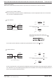
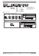
Method to cancel each command
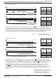
READ
Fig.48 READ cancel valid timing
RDSR
Fig.49 RDSR cancel valid timing
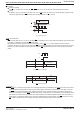
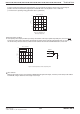
WRSR
Fig.51 WRSR cancel valid timing
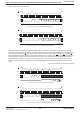
WRITE, PAGE WRITE
Fig.50 WRITE cancel valid timing
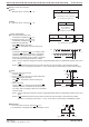
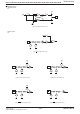
WREN/WRDI
Fig.52 WREN / WRDI cancel valid timing
8 bits 8 bits
Data
Cancel available in all areas of read mode
Ope code
8 bits 8 bits
Cancel available in all
areas of read mode
Ope code Data
a b
d
c
tE/W
8 bits 8 bits 8 bits
Ope code Address
Data (n)
¢ Method to cancel : cancel by CS = "H"
¢
Method to cancel : cancel by CS = "H"
a
c
b
tE/W
8 bit 8 bit
Ope code
Address
b
SCK
SI
D1 D0
15 16 1714
ca
b
c
SCK
SI
D7 D6 D5 D4 D3
D2 D1 D0
ba
8 bit
b
SCK
897
a
Ope code
Note 1) If Vcc is made OFF during write execution, designated address data is not guaranteed, therefore write it once
again.
Note 2) If CS is started at the same timing as that of the SCK rise, write execution / cancel becomes unstable,
therefore, it is necessary to fall in SCK = "L" area. As for SCK rise, assure timing of tCSS / tCSH or higher.
a : Ope code, address input area.
Cancellation is available by CS = "H".
b : Data input area (D7 ~ D1 input area)
Cancellation is available by CS = "H".
c : Data input area (D0 area)
When CS is started, write starts.
After CS rise, cancellation cannot be made by any
means.
d : tE/W area
Cancellation is available by CS = "H". However, when
write starts (CS is started) in the area c, cancellation
cannot be made by any means. And, by inputting on
SCK clock, cancellation cannot be made. In page write
mode, there is write enable area at every 8 clocks.
a : From ope code to 15 clock rise
Cancel by CS = "H".
b : From 15 clock rise to 16 clock rise (write enable area)
When CS is started, write starts.
After CS rise, cancellation cannot be made by any
means.
c : After 16 clock rise
Cancel by CS = "H". However, when write starts (CS is
started) in the area b, cancellation cannot be made by
any means. And, by inputting on SCK clock, cancellation
cannot be made.
Note 1) If Vcc is made OFF during write execution, designated address data is not guaranteed, therefore write it once
again.
Note 2) If CS is started at the same timing as that of the SCK rise, write execution / cancel becomes unstable,
therefore, it is necessary to fall in SCK = "L" area. As for SCK rise, assure timing of tCSS/tCSH or higher.
a : From ope code to clock rise, cancel by CS = "H".
b : Cancellation is not available when CS is started after 7 clock.
8 bits /16 bits
Address
2010.07 -
Rev. B
www.rohm.com
© 2010 ROHM Co., Ltd. All rights reserved.