
Datasheet

Technical Note
18/21
BR24T□□□-W Series
www.rohm.com
2011.1 - Rev.H
© 2011 ROHM Co., Ltd. All rights reserved.
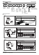
●Notes on power ON
At power on, in IC internal circuit and set, Vcc rises through unstable low voltage area, and IC inside is not completely reset, and
malfunction may occur. To prevent this, functions of POR circuit and LVCC circuit are equipped. To assure the action, observe the following
conditions at power on.
1. Set SDA = 'H' and SCL ='L' or 'H’
2. Start power source so as to satisfy the recommended conditions of t
R
, t
OFF
, and Vbot for operating POR circuit.
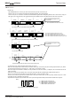
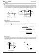
tOFF
tR
Vbot
0
V
CC
3. Set SDA and SCL so as not to become 'Hi-Z'.
When the above conditions 1 and 2 cannot be observed, take the following countermeasures.
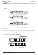
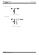
a) In the case when the above condition 1 cannot be observed. When SDA becomes 'L' at power on .
→Control SCL and SDA as shown below, to make SCL and SDA, 'H' and 'H'.
b) In the case when the above condition 2 cannot be observed.
→After power source becomes stable, execute software reset(P12).
c) In the case when the above conditions 1 and 2 cannot be observed.
→Carry out a), and then carry out b).
● Low voltage malfunction prevention function
LVCC circuit prevents data rewrite action at low power, and prevents wrong write. At LVCC voltage (Typ. =1.2V) or below, it prevent data
rewrite.
●Vcc noise countermeasures
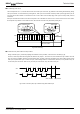
○Bypass capacitor
When noise or surge gets in the power source line, malfunction may occur, therefore, for removing these, it is recommended to attach a by
pass capacitor (0.1μF) between IC Vcc and GND. At that moment, attach it as close to IC as possible.
And, it is also recommended to attach a bypass capacitor between board Vcc and GND.
● Cautions on use
(1)
Described numeric values and data are design representative values, and the values are not guaranteed.
(2) We believe that application circuit examples are recommendable, however, in actual use, confirm characteristics further sufficiently. In the
case of use by changing the fixed number of external parts, make your decision with sufficient margin in consideration of static
characteristics and transition characteristics and fluctuations of external parts and our LSI.
(3)
Absolute maximum ratings
If the absolute maximum ratings such as impressed voltage and action temperature range and so forth are exceeded, LSI may be
destructed. Do not impress voltage and temperature exceeding the absolute maximum ratings. In the case of fear exceeding the absolute
maximum ratings, take physical safety countermeasures such as fuses, and see to it that conditions exceeding the absolute maximum
ratings should not be impressed to LSI.
(4) GND electric potential
Set the voltage of GND terminal lowest at any action condition. Make sure that each terminal voltage is lower than that of GND terminal.
(5) Terminal design
In consideration of permissible loss in actual use condition, carry out heat design with sufficient margin.
(6) Terminal to terminal shortcircuit and wrong packaging
When to package LSI onto a board, pay sufficient attention to LSI direction and displacement. Wrong packaging may destruct LSI. And in
the case of shortcircuit between LSI terminals and terminals and power source, terminal and GND owing to foreign matter, LSI may be
destructed.
(7)
Use in a strong electromagnetic field may cause malfunction, therefore, evaluate design sufficiently.
Fig.56 Rise waveform diagram
tLOW
tSU:DAT tDH
A
fter Vcc becomes stable
SCL
VCC
SDA
Fi
g
.57 When SCL= 'H' and SDA= 'L'
tSU:DAT
A
fter Vcc becomes stable
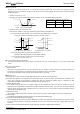
Fi
g
.58 When SCL='L' and SDA='L'
Recommended conditions of tR, tOFF,Vbot
tR tOFF Vbot
10ms or belo
w
10ms or larger 0.3V or below
100 or below 10ms or larger 0.2V or below