
Datasheet

BD9701FP/CP-
V
5/T/
T
-
V
5,BD9703FP/CP-
V
5/T/
T
-
V
5,BD9702CP-
V
5/T/
T
-
V
5
Technical Note
9/16
www.rohm.com
2009.04- Rev.B
© 2009 ROHM Co., Ltd. All rights reserved.
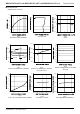
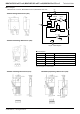
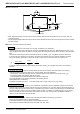
●Notes for PCB layout
Fig.30 Layout
• Place capacitors between VCC and Ground, and the Schottky diode as close as possible to the IC to reduce noise and
maximize efficiency.
• Connect resistors between INV and Ground, and the output capacitor filter at the same Ground potential in order to stabilize
the output voltage.
●Application component selection and settings
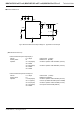
Inductor L1
If the winding resistance of the choke coil is too high, the efficiency may deteriorate.
As the overcurrent protection operates over minimum 1.6A (BD9701FP/CP-V5/T/T-V5, BD9703FP/CP-V5/T-V5) or 3.2A
minimum (BD9701CP-V5/T/T-V5), attention must be paid to the heating of the inductor due to overload of short-circulated
load.
Note that the current rating for the coil should be higher than I
OUT
(MAX)+⊿IL
.
Iout (MAX): maximum load current
If you flow more than maximum current rating, coil will become overload, and cause magnetic saturation, and those
account for efficiency deterioration. Select from enough current rating of coil which doesn’t over peak current.
L1:inductor value, VCC:maximum input voltage, VOUT:output voltage, ⊿IL:coil ripple current value, fosc:oscillation
frequency
Shottky Barrier Diodes D1
A Schottky diode with extremely low forward voltage should be used. Selection should be based on the following
guidelines regarding maximum forward current, reverse voltage, and power dissipation:
・The maximum current rating is higher than the combined maximum load current and coil ripple current (⊿I
L
).
・The reverse voltage rating is higher than the VIN value.
・Power dissipation for the selected diode must be within the rated level.
The power dissipation of the diode is expressed by the following formula:
Pdi=Iout(MAX)×Vf×(1-VOUT/VCC)
Iout (MAX): maximum load current, Vf: forward voltage, VOUT: output voltage, VCC: input voltage
Capacitor C1,C2,C3,C4,C5
As large ripple currents flow across C1 and C3 capacitors, high frequency and low impedance capacitor for a switching
regulator must be used. The ceramic capacitor C2 must be connected. If not, noise may cause an abnormal operation. If
the ripple voltage of input and output is large, C4 selected among ceramic , tantalum and OS capacitor with low ESR may
decrease the ripple, however if the only low ESR capacitor is used, an oscillation or unstable operation may be caused.
C5 is the capacitor for phase compensation and normally not used. If you need to improve the stability of feedback
network, connect C5 between INV and OUTPUT.
Feed back resistance R1,R2
The offset of output voltage is determined by both Feed back resistance and INV pin input current.
VOUT=(R1+R2) VINV/R2 (VINV pin Threshold Votage)
If Feed back resistance is high, the setting of output voltage will be move.
Recommended : Resistance between INV pin and GND = less than 10kΩ.
⊿IL
.
=
L1
(VCC-VOUT)
VOUT
VCC
fosc
1
× ×
4
5
2
3
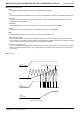
1
INV
STBY
R2 : 1kO
R1 : 4kO
C5
VCC
OUT
GND
C2
5.0V
L1
D1
C3
C4
C1