
Datasheet

BD9701FP/CP-
V
5/T/
T
-
V
5,BD9703FP/CP-
V
5/T/
T
-
V
5,BD9702CP-
V
5/T/
T
-
V
5
Technical Note
8/16
www.rohm.com
2009.04- Rev.B
© 2009 ROHM Co., Ltd. All rights reserved.
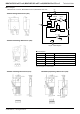
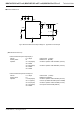
●Block Function Explanations
・VREF
Generates the regulated voltage from VCC input, compensated for temperature.
・OSC
Generates the triangular wave oscillation frequency using an internal resistors and capacitor. Used for PWM comparator input.
・Error AMP
This block, via the INV pin, detects the resistor-divided output voltage, compares this with the reference voltage, then
amplifies and outputs the difference.
・PWM COMP
Outputs PWM signals to the Driver block, which converts the error amp output voltage to PWM form.
・DRIVER
This push-pull FET driver powers the internal Pch MOSFET, which accepts direct PWM input.
・STBY
Controls ON/OFF operation via the STBY pin. The output is ON when STBY is High.
・Thermal Shutdown (TSD)
This circuit protects the IC against thermal runaway and damage due to excessive heat. A thermal sensor detects the
junction temperature and switches the output OFF once the temperature exceeds a threshold value (175deg). Hysteresis
is built in (15deg) in order to prevent malfunctions due to temperature fluctuations.
・Over Current Protection (OCP)
The OCP circuit detects the voltage difference between VCC and OUT by measuring the current through the internal Pch
MOSFET and switches the output OFF once the voltage reaches the threshold value. The OCP block is a self-recovery
type (not latch).
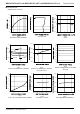
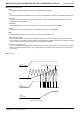
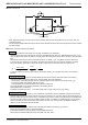
●Timing Chart
Error AMP OUTPUT
OUTPIN
OSC
(Internal Oscillation Wave)
OUTPUT
VCC PIN
VOLTAGE WAVE
VOLTAGE WAVE
VOLTAGE WAVE
Fig.29 Timing Chart