
Datasheet
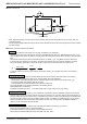

BD9701FP/CP-
V
5/T/
T
-
V
5,BD9703FP/CP-
V
5/T/
T
-
V
5,BD9702CP-
V
5/T/
T
-
V
5
Technical Note
3/16
www.rohm.com
2009.04- Rev.B
© 2009 ROHM Co., Ltd. All rights reserved.
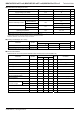
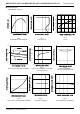
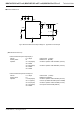
●Electrical Characteristics
○BD9703FP/CP-V5/T/T-V5 (Unless otherwise noted, Ta=25℃,VCC=12V,Vo=5V,STBY=3V)
Parameter Symbol
Limit
Unit Conditions
MIN TYP MAX
Output ON Resistance Ron - 1.0 1.5 Ω design guarantee
Efficiency η - 86 - % Io=0.5A design guarantee
Switching Frequency fosc 270 300 330 kHz
Load Regulation ΔVOLOAD - 10 40 mV VCC=20V,Io=0.5~1.5A
Line Regulation ΔVOLINE - 40 100 mV VCC=10~30V,Io=1.0A
Over Current Protection Limit Iocp 1.6 - - A
INV Pin Threshold Voltage VINV 0.98 1.00 1.02 V
INV Pin Threshold Voltage
Thermal Variation
ΔVINV - ±0.5 - % Tj=0~85℃ design guarantee
INV Pin Input Current IINV - 1 - μA VINV=1.0V
STBY Pin
Threshold Voltage
ON
VSTBYON 2.0 - 36
V
OFF
VSTBYOFF -0.3 - 0.3
V
STBY Pin Input Current Istby 5 25 50 μASTBY=3V
Circuit Current Icc - 5 12 mA
Stand-by Current Ist - 0 5 μASTBY=0V
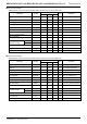
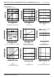
●Electrical Characteristics
○BD9702FP/CP-V5/T/T-V5 (Unless otherwise noted, Ta=25℃,VCC=12V,Vo=5V,STBY=3V)
Parameter Symbol
Limit
Unit Conditions
MIN TYP MAX
Output ON Resistance Ron - 0.5 1.5 Ω design guarantee
Efficiency η - 86 - % Io=1A design guarantee
Switching Frequency fosc 88 110 132 kHz
Load Regulation ΔVOLOAD - 10 40 mV VCC=20V,Io=1~3A
Line Regulation ΔVOLINE - 40 100 mV VCC=10~30V,Io=1.0A
Over Current Protection Limit Iocp 3.2 - - A
INV Pin Threshold Voltage VINV 0.98 1.00 1.02 V
INV Pin Threshold Voltage
Thermal Variation
ΔVINV - ±0.5 - % Tj=0~85℃ design guarantee
INV Pin Input Current IINV - 1 - μA VINV=1.0V
STBY Pin
Threshold Voltage
ON
VSTBYON 2.0 - 36 V
OFF
VSTBYOFF -0.3 - 0.3 V
STBY Pin Input Current Istby 5 25 50 μASTBY=3V
Circuit Current Icc - 4 12 mA
Stand-by Current Ist - 0 5 μASTBY=0V