
Datasheet
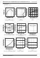

BD9701FP/CP-
V
5/T/
T
-
V
5,BD9703FP/CP-
V
5/T/
T
-
V
5,BD9702CP-
V
5/T/
T
-
V
5
Technical Note
2/16
www.rohm.com
2009.04- Rev.B
© 2009 ROHM Co., Ltd. All rights reserved.
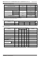
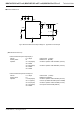
●Absolute Maximum Ratings (Ta=25℃)
Parameter Symbol Ratings Unit
Supply Voltage (VCC-GND) VCC 36 V
STBY-GND V
STBY
36 V
OUT-GND V
O
36 V
INV-GND V
INV
10 V
Maximum Switching Current
BD9701/BD9703
Iout
1.5
A
BD9702 3
Power Dissipation
TO252
Pd
0.8
(*1)
W
TO220 2
(*2)
Operating Temperature Topr -40~+85 ℃
Storage Temperature Tstg -55~+150 ℃
*1 Without external heat sink, the power dissipation reduces by 6.4mW/℃ over 25℃.
*2 Without external heat sink, the power dissipation reduces by 16.0mW/℃ over 25℃.
Reduced by 160mW/℃, when mounted on Infinity size heatsink.
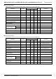
●Operating Conditions(Ta=-40~+85℃)
Parameter Symbol
Limit
Unit
MIN TYP MAX
Input Voltage VCC 8.0 or Vo+3
(*3)
- 35.0 V
Output Voltage Vo 1.0 - 32 V
*3The minimum value of an input voltage is the higher either 8.0V or Vo+3
●Electrical Characteristics
○BD9701FP/CP-V5/T/T-V5 (Unless otherwise noted, Ta=25℃,VCC=12V,Vo=5V,STBY=3V)
Parameter Symbol
Limit
Unit Conditions
MIN TYP MAX
Output ON Resistance Ron - 1.0 1.5 Ω design guarantee
Efficiency η - 86 - % Io=0.5A design guarantee
Switching Frequency fosc 80 100 120 kHz
Load Regulation ΔVOLOAD - 10 40 mV VCC=20V,Io=0.5~1.5A
Line Regulation ΔVOLINE - 40 100 mV VCC=10~30V,Io=1.0A
Over Current Protection Limit Iocp 1.6 - - A
INV Pin Threshold Voltage VINV 0.98 1.00 1.02 V
INV Pin Threshold Voltage
Thermal Variation
ΔVINV - ±0.5 - % Tj=0~85℃ design guarantee
INV Pin Input Current IINV - 1 - μA VINV=1.0V
STBY Pin
Threshold Voltage
ON
VSTBYON 2.0 - 36 V
OFF
VSTBYOFF -0.3 - 0.3 V
STBY Pin Input Current Istby 5 25 50 μASTBY=3V
Circuit Current Icc - 4 12 mA
Stand-by Current Ist - 0 5 μASTBY=0V
This product is not designed to be resistant to radiation.