
Datasheet

BD9701FP/CP-
V
5/T/
T
-
V
5,BD9703FP/CP-
V
5/T/
T
-
V
5,BD9702CP-
V
5/T/
T
-
V
5
Technical Note
13/16
www.rohm.com
2009.04- Rev.B
© 2009 ROHM Co., Ltd. All rights reserved.
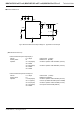
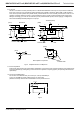
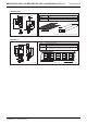
Output Pin
VCC
Back current prevention diode
Bypass diode
8. IC pin input
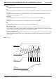
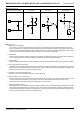
This IC is a monolithic IC which (as below) has P+ substrate and betweenthe various pin. A P-N junction is formed from
this P layer of each pin. For example the relation between each potential is as follows. (When GND > PinB and GND >
PinA, the P-N junction operates as a parasitic diode.) Parasitic diodes can occur inevitably in the structure of the IC. The
operation of parasitic diodes can result in mutual interference among circuits as well as operation faults and physical
damage. Accordingly, you must not use methods by which parasitic diodes operate, such as applying a voltage that is
lower than the GND(P substrate)voltage to an input pin.
9. Common impedance
Power supply and ground wiring should reflect consideration of the need to lower common impedance and minimize ripple
as much as possible (by making wiring as short and thick as possible or rejecting ripple by incorporating inductance and
capacitance).
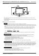
10. Pin short and mistake fitting
Do not short-circuit between OUT pin and VCC pin, OUT pin and GND pin,
or VCC pin and GND pin. When soldering the IC on circuit board,
please be unusually cautious about theorientation and the position of the IC.
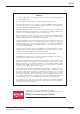
Fig.35
P substrate
N
Parasitic diode
~
~
GND
N
P
N
P
+
P
+
Resistance
Parasitic diode
~
~
GND
N
P
N N
P
+
P
+
Transistor (NPN)
B
N
E
C
GND
P substrate
~
~
GND
B
C
E
Other adjacent components
Parasitic diode
~
~
GND
Parasitic diode
(PinB)
(PinA)
(PinB)
(PinA)
Fig.34 Simplified structure of a Bipolar IC