
Datasheet

BD9701FP/CP-
V
5/T/
T
-
V
5,BD9703FP/CP-
V
5/T/
T
-
V
5,BD9702CP-
V
5/T/
T
-
V
5
Technical Note
12/16
www.rohm.com
2009.04- Rev.B
© 2009 ROHM Co., Ltd. All rights reserved.
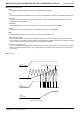
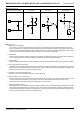
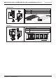
●I/O Equivalent Circuit
Pin 1 (VCC), Pin 3 (GND) Pin 2 (OUT) Pin 4 (INV) Pin 5 (STBY)
●Notes for use
1. Absolute Maximum Ratings
Use of the IC in excess of absolute maximum ratings such as the applied voltage or operating temperature range may
result in IC deterioration or damage. Assumptions should not be made regarding the state of the IC (short mode or open
mode) when such damage is suffered. A physical safety measure such as a fuse should be implemented when use of the
IC in a special mode where the absolute maximum ratings may be exceeded is anticipated.
2. GND voltage
Ensure a minimum GND pin potential in all operating conditions. In addition, ensure that no pins other than the GND pin
carry a voltage lower than or equal to the GND pin, including during actual transient phenomena.
3. Thermal design
Use a thermal design that allows for a sufficient margin in light of the power dissipation (Pd) in actual operating conditions.
4. Inter-pin shorts and mounting errors
Use caution when orienting and positioning the IC for mounting on printed circuit boards. Improper mounting may result in
damage to the IC. Shorts between output pins or between output pins and the power supply and GND pin caused by the
presence of a foreign object may result in damage to the IC.
5. Operation in strong electromagnetic field
Operation in a strong electromagnetic field may cause malfunction.
6. Thermal shutdown circuit (TSD circuit)
This IC incorporates a built-in thermal shutdown circuit (TSD circuit). The TSD circuit is designed only to shut the IC off to
prevent runaway thermal operation. Do not continue to use the IC after operating this circuit or use the IC in an
environment where the operation of the thermal shutdown circuit is assumed.
7. Testing on application boards
When testing the IC on an application board, connecting a capacitor to a pin with low impedance subjects the IC to stress.
Always discharge capacitors after each process or step. Ground the IC during assembly steps as an antistatic measure,
and use similar caution when transporting or storing the IC. Always turn the IC's power supply off before connecting it to or
removing it from a jig or fixture during the inspection process.
VCC
GND
OUT
VCC
INV
VCC
300Ω
STB
VC
70KΩ
60KΩ
140KΩ
Fig.33Input Output Equivalent Circuit