
Datasheet

BD9540EFV
Technical Note
4/17
www.rohm.com
2009.04 - Rev.B
© 2009 ROHM Co., Ltd. All rights reserved.
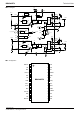
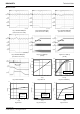
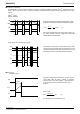
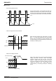
●Pin Function
PIN No. PIN name PIN Function
1 BOOT1 HG Driver Power Supply Pin 1
2 NC Non connection Pin
3 EN1 Enable Input Pin 1 (0~0.3V:OFF, 2.2~20V:ON)
4 VOUT1 Output Voltage Sence Pin 1
5 FB1 Output Voltage Feedback Pin 1
6 NC Non connection Pin
7 GND Sense GND
8 CTL1 1ch Reference Voltage Setting Control Pin 1:See P12/17
9 CTL2 1ch Reference Voltage Setting Control Pin 2:See P12/17
10 FB2 Output Voltage Feedback Pin 2
11 VOUT2 Output Voltage Sense Pin 2
12 EN2 Enable Input Pin 2 (0~0.3V:OFF, 2.2~20V:ON)
13 NC Non connection Pin
14 BOOT2 HG Driver Power Supply Pin 2
15 HG2 High side FET Gate Driver Pin 2
16 SW2 High side FET Source Pin 2
17 LG2 Low side FET Gate Driver Pin 2
18 PGND2 Power GND for 2ch
19 ILIM2 2ch OCP Setting Pin
20 TEST Connect to GND Pin
21 VCC Power Supply Input Pin
22 5VReg Reference Voltage Inside IC (5V Voltage Output)
23 VIN Battery Voltage Sense Pin
24 ILIM1 1ch OCP Setting Pin
25 PGND1 Power GND for 1ch
26 LG1 Low side FET Gate Driver Pin 1
27 SW1 High side FET Source Pin 1
28 HG1 High side FET Gate Driver Pin 1
reverse FIN Exposed Pad, Connect to GND