
Datasheet

BD9540EFV
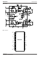
Technical Note
2/17
www.rohm.com
2009.04 - Rev.B
© 2009 ROHM Co., Ltd. All rights reserved.
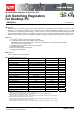
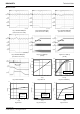
●Operating Conditions (Ta=25℃)
Parameter Symbol Min. Max. Unit
Input voltage VIN 7.5 20 V
BOOT voltage BOOT1, BOOT2 4.5 25 V
SW Voltage SW1, SW2 -0.7 20 V
BOOT-SW voltage BOOT1-SW1, BOOT2-SW2 4.5 5.5 V
Logic Input Voltage 1 EN1, EN2 0 20 V
Logic Input Voltage 2 CTL1, CTL2 0 5.5 V
Output Voltage VOUT1, VOUT2 0.7 5.5 V
MIN ON Time tonmin - 100 ns
*This product should not be used in a radioactive environment.
*The range of the VOUT is limited by the voltage between VIN and VOUT.
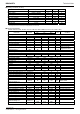
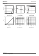
●Electrical characteristics
(Unless otherwise noted, Ta=25℃ VCC=5V, VIN=12V, VEN1=VEN2=3V, Vout1=1.5V, Vout2=1.05V)
Parameter Symbol
Limit
Unit Condition
Min. Typ. Max.
[General]
VIN Bias Current IIN - 1.6 2.5 mA
VIN Standby Current IIN_stb - 0 10 A VEN1=VEN2=0V
EN Low Voltage 1,2 VEN_low1,2 GND - 0.3 V
EN High Voltage 1,2 VEN_high1,2 2.2 - 20 V
EN Bias Current 1,2 IEN1,2 - 1.5 5.0 A VEN1=VEN2=3V
[5V Linear Regulator]
5VReg Standby Voltage 5Vreg_stb - - 0.1 V VEN1=VEN2=0V
5VReg Output Voltage 5VReg 4.8 5.0 5.2 V
VIN=7.5V to 20V
Ireg=0mA to 10mA
Maximum Current IReg 50 - - mA
[Under-Voltage Lock-Out]
5VReg Threshold Voltage 5Vreg_UVLO 3.75 4.20 4.65 V 5VReg:Sweep up
5VReg Hysteresis Voltage d5Vreg_UVLO 100 160 220 mV 5VReg:Sweep down
[OVP Block]
FB Threshold Voltage 1 FB_OVP1 0.92 1.02 1.12 V
FB Threshold Voltage 2 FB_OVP2 0.80 0.90 1.00 V
OVP delay time tOVP - 1.7 - s
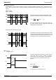
[H
3
Reg
TM
Control Block]
ON Time1 ton1 290 390 490 ns
MIN OFF Time 1 toffmin1 200 380 - ns
ON Time 2 ton2 110 210 310 ns
MIN OFF Time 2 toffmin2 200 380 - ns
[FET Block]
HG High side ON Resistance 1,2 RHGhon1,2 - 5.5 11
HG Low side ON Resistance 1,2 RHGlon1,2 - 2.5 5
LG High side ON Resistance 1,2 RLGhon1,2 - 4 8
LG Low side ON Resistance 1,2 RLGlon1,2 - 2 4
[Over Current Protection Block]
Current Limit
Threshold Voltage 1,2
Vilim1,2 80 100 120 mV RILIM=100k
[Output Voltage Detection Block]
FB1 threshold(REF1) Voltage1 FB1-1 0.769 0.781 0.793 V CTL1=0V, CTL2=0V
FB1 threshold(REF1) Voltage2 FB1-2 0.802 0.814 0.826 V CTL1=5V, CTL2=0V
FB1 threshold(REF1) Voltage3 FB1-3 0.839 0.851 0.863 V CTL1=0V, CTL2=5V
FB1 threshold(REF1) Voltage4 FB1-4 0.738 0.750 0.762 V CTL1=5V, CTL2=5V
FB2 threshold(REF2) Voltage FB2 0.738 0.750 0.762 V
CTL Low Voltage 1,2 VCTL_low1,2 GND - 0.5 V
CTL High Voltage 1,2 VCTL_high1,2 VCC-0.5 - VCC V
FB1/2 Input Current IFB1,2 -1 - 1 A
VOUT Discharge Current IVOUT1,2 5 10 - mA VOUT=1V, EN=0V
[SCP Block]
Threshold Voltage 1,2 Vthscp1,2
REF1,2×
0.60
REF1,2×
0.70
REF1,2×
0.80
V
SCP delay time tSVP - 28 - s