
Datasheet

BD9540EFV
Technical Note
12/17
www.rohm.com
2009.04 - Rev.B
© 2009 ROHM Co., Ltd. All rights reserved.
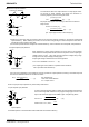
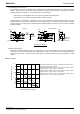
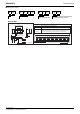
6. Output Voltage Setting
The IC will try to maintain output voltage such that REF≒VFB.
However, the actual output voltage will also reflect the average ripple voltage value.
The output voltage is set via a resistive voltage divider between the output and the FB pin. The formula for output voltage
is given in (13) below:
Output voltage= ×
It is recommended that R1 and C1 be connected in parallel to the FB pin.
In low output ripple applications (V < 20 mV), add Radd and Cadd as shown in the above application circuit.
For value settings, refer to the tool provided separately.
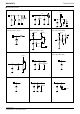
REF voltage (for 2ch) is fixed at 0.750 V; however, REF voltage (for 1ch) can be adjusted via the CTL input conditions.
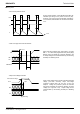
REF1 voltage setting table
CTL1 CTL2 REF1
L L 0.781V
H L 0.814V
L H 0.851V
H H 0.750V
R1+R2
R2
1
2
REF + ×I
L×ESR・・・(13)
H
3
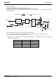
Reg
TM
CONTROLLA
S
RQ
Driver
Circuit
Output voltage
FB
R1
R2
ESR
REF
VIN
C1
Cadd (for Low Ripple)
Radd (for Low Ripple)