
Datasheet


BD9540EFV
Technical Note
11/17
www.rohm.com
2009.04 - Rev.B
© 2009 ROHM Co., Ltd. All rights reserved.
4. MOSFET Selection
5. Determining Detection Resistance
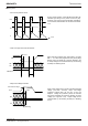
Pmain = P
RON + PGATE + PTRAN
Psyn = P
RON + PGATE
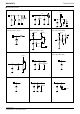
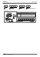
V
IN-VOUT
VIN
×RON×IOUT
2
+5VReg×f×VDD
VIN
L
Co
V
OUT
synchronous switch
main switch
Main MOSFET power dissipation is computed as follows:
(Ron: On-resistance of FET; Qg: FET gate capacitance;
f: Switching frequency; Crss: FET inverse transfer function;
I
DRIVE
: Gate peak current)
Synchronous MOSFET power dissipation is computed as follows:
=
・・・(10)
V
OUT
VIN
×RON×IOUT
2
+Qg(High)×f×5VReg+
V
IN
2
×Crss×IOUT×f
I
DRIVE
= ・・・(9)
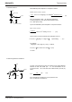
Qg loss is also incurred as internal power dissipation in the IC:
For example:
If Qg(High) = 20nq, Qg(Low) = 50nq, f = 300kHz,
P
IC(DRIVE) = Qg(High)×f + Qg(Low)×f ×(VIN-5VReg) ・・・(11)
=
PIC(DRIVE) = 20n×300k +50n×300k ×(12-5)
= 0.147W
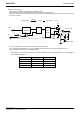
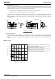
The over-current protection function is controlled via the voltage detected
between the SW and PGND pins – i.e., the ON-resistance of the
synchronous FET. The current limit value is determined by formula (12)
below:
10k
R
ILIM ×RON
ILIM=
(R
ILIM: Resistance for setting over-current protection limit,
RON: Low side FET On-resistance)
VIN
L
Co
VOUT
[A]・・・(12)
PGND
SW
RILIM