
Datasheet

Technical Note
5/9
BD52□□G, BD52□□FVE, BD53□□G, BD53□□FVE series
www.rohm.com
2009.06 - Rev.B
© 2009 ROHM Co., Ltd. All rights reserved.
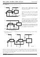
Setting of Detector Delay Time
This detector IC can be set delay time at the rise of V
DD by the capacitor connected to CT terminal.
Delay time at the rise of V
DD
T
PLH
:Time until when Vout rise to 1/2 of V
DD
after V
DD
rise up and beyond the release
voltage(V
DET
+V
DET
)
T
PLH
= -C
CT
×R
CT
×ln
C
CT
: CT pin Externally Attached Capacitance R
CT
: CT pin Internal Impedance (P.2 R
CT
refer.)
V
CTH
: CT pin Threshold Voltage(P.2 VCTH refer.) Ln : Natural Logarithm
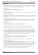
Reference Data of Falling Time (T
PHL
) Output
Examples of Falling Time (T
PHL
) Output
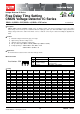
Part Number tPHL[µs] -40°C tPHL[µs] ,+25°C tPHL[µs],+105°C
BD5227G 30.8 30 28.8
BD5327G 26.8 26 24.8
*This data is for reference only.
The figures will vary with the application, so please confirm actual operating conditions before use.
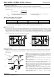
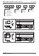
Explanation of Operation
For both the open drain type (Fig.15) and the CMOS output type (Fig.16), the detection and release voltages are used as
threshold voltages. When the voltage applied to the VDD pins reaches the applicable threshold voltage, the VOUT terminal
voltage switches from either “High” to “Low” or from “Low” to “High”. Because the BD52G/FVE series uses an open drain
output type, it is possible to connect a pull-up resistor to VDD or another power supply [The output “High” voltage (VOUT) in
this case becomes VDD or the voltage of the other power supply].
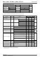
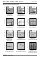
Fig.15 (BD52Type Internal Block Diagram) Fig.16 (BD53Type Internal Block Diagram)
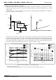
Timing Waveforms
Example: the following shows the relationship between the input voltage V
DD, the CT Terminal Voltage VCT and the output
voltage
VOUT when the input power supply voltage VDD is made to sweep up and sweep down (The circuits are those in
Fig.15 and 16).
1
When the power supply is turned on, the output is unsettled from
after over the operating limit voltage (V
OPL) until TPHL. There fore it is
possible that the reset signal is not outputted when the rise time of
VDD is faster than T
PHL.
2
When VDD is greater than VOPL but less than the reset release
voltage (V
DET+VDET), the CT terminal (VCT) and output (VOUT)
voltages will switch to L.
3
If VDD exceeds the reset release voltage (VDET+VDET), then
V
OUT switches from L to H (with a delay to the CT terminal).
4
If VDD drops below the detection voltage (VDET) when the power
supply is powered down or when there is a power supply fluctuation,
V
OUT switches to L (with a delay of TPHL).
5
The potential difference between the detection voltage and the
release voltage is known as the hysteresis width (V
DET). The
system is designed such that the output does not flip-flop with power
supply fluctuations within this hysteresis width, preventing
malfunctions due to noise.
Vref
V
DD
GND
CT
R1
R2
R3
Q3
Q1
V
OUT
RESET
R
L
V
DD
Vref
V
DD
GND
CT
R1
R2
R3
Q3
Q2
V
OUT
RESET
Q1
V
DD
V
DD
V
DET
+
Δ
V
DET
V
DET
V
OPL
0V
1/2 V
DD
T
PHL
①
T
PLH
T
PHL
T
PLH
② ③ ④
V
CT
⑤
V
OUT
Fig.17
V
DD
-V
CTH
V
DD