
Datasheet

Technical Note
2/9
BD52□□G, BD52□□FVE, BD53□□G, BD53□□FVE series
www.rohm.com
2009.06 - Rev.B
© 2009 ROHM Co., Ltd. All rights reserved.
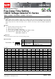
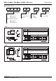
Absolute maximum ratings (Ta=25°C)
Parameter Symbol Limits Unit
Power Supply Voltage VDD-GND -0.3 ~ +10 V
Output Voltage
Nch Open Drain Output
VOUT
GND-0.3 ~ +10
V
CMOS Output GND-0.3 ~ VDD+0.3
Power
Dissipation
SSOP5
*1*3
Pd
540
mW
VSOF5
*2*3
210
Operating Temperature Topr -40 ~ +105 °C
Ambient Storage Temperature Tstg -55 ~ +125 °C
*1 Use above Ta=25°C results in a 5.4mW loss per degree.
*2 Use above Ta=25°C results in a 2.1mW loss per degree.
*3 When a ROHM standard circuit board (70mm×70mm×1.6mm glass epoxy board) is mounted.
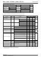
Electrical characteristics (Unless Otherwise Specified Ta=-40 to 105°C)
Parameter Symbol Condition
Limit
Unit
Min. Typ. Max.
Detection Voltage V
DET
VDD=HL, RL=470k
*1
V
DET(T)
×0.99
V
DET(T)
V
DET(T)
×1.01
V
Circuit Current when ON IDD1 VDD=VDET-0.2V
V
DET
=2.3-3.1V - 0.80 2.40
µA
V
DET
=3.2-4.2V - 0.85 2.55
V
DET
=4.3-5.2V - 0.90 2.70
V
DET
=5.3-6.0V - 0.95 2.85
Circuit Current when OFF IDD2 VDD=VDET+2.0V
V
DET
=2.3-3.1V - 0.75 2.25
µA
V
DET
=3.2-4.2V - 0.80 2.40
V
DET
=4.3-5.2V - 0.85 2.55
V
DET
=5.3-6.0V - 0.90 2.70
Operating Voltage Range VOPL
VOL0.4V, Ta=25~105°C, RL=470k 0.95 - -
V
VOL0.4V, Ta=-40~25°C, RL=470k 1.20 - -
‘Low’ Output Current (Nch) IOL
V
DS=0.5V VDD=1.2V 0.4 1.2 -
mA
VDS=0.5V VDD=2.4V 2.0 5.0 -
‘High’ Output Current (Pch) IOH
V
DS=0.5V VDD=4.8V VDET=2.3-4.2V 0.7 1.4 -
mA
VDS=0.5V VDD=6.0V VDET=4.3-5.2V 0.9 1.8 -
VDS=0.5V VDD=8.0V VDET=5.3-6.0V 1.1 2.2 -
Leak Current when OFF Ileak VDD=VDS=10V
*1
- - 0.1 µA
CT pin Threshold Voltage VCTH
V
DD=VDET×1.1, VDET=2.3-2.6V, RL=470k
V
DD
×0.30
VDD
×0.40
VDD
×0.60
V
VDD=VDET×1.1, VDET=2.7-4.2V, RL=470k
VDD
×0.30
VDD
×0.45
VDD
×0.60
VDD=VDET×1.1, VDET=4.3-5.2V, RL=470k
V
DD
×0.35
VDD
×0.50
VDD
×0.60
VDD=VDET×1.1, VDET=5.3-6.0V, RL=470k
VDD
×0.40
VDD
×0.50
VDD
×0.60
Output Delay Resistance RCT VDD=VDET×1.1 VCT=0.5V
*1
5.5 9 12.5 M
CT pin Output Current ICT
VCT=0.1V VDD=0.95V
*1
15 40 -
µA
VCT=0.5V VDD=1.5V 150 240 -
Detection Voltage
Temperature coefficient
VDET/T Ta=-40°C to 105°C - ±100 ±360 ppm/°C
Hysteresis Voltage VS VDD=LHL, RL=470k
V
DET
×0.03
VDET
×0.05
VDET
×0.08
V
V
S
(T) : Standard Detection Voltage (2.3V to 6.0V, 0.1V step)
R
L
: Pull-up resistor to be connected between VOUT and power supply.
Designed Guarantee. (Outgoing inspection is not done on all products.)
*1 Guarantee is Ta=25°C.