
Datasheet


Technical Note
BA10358F/FV, BA10324AF/FV, BA2904SF/FV/FVM, BA2904F/FV/FVM
BA2902SF/FV/KN, BA2902F/FV/KN, BA3404F/FVM
22/25
www.rohm.com
2010.11 - Rev.
A
© 2010 ROHM Co., Ltd. All rights reserved.
0
200
400
600
800
1000
0 25 50 75 100 125
周囲温度
Ta
[
℃
]
許容損失
Pd
[mW]
BA10358F
BA10358FV
620mW (*1)
550mW (*2)
(a) BA10358 ファミリ
0
200
400
600
800
1000
0 25 50 75 100 125
周囲温度
Ta
[
℃
]
許容損失
Pd
[mW]
BA10324AFV
BA10324AF
700mW (*3)
490mW (*4)
(a) BA10324A ファミリ
0
200
400
600
800
1000
0 25 50 75 100 125 150
周囲温度
Ta
[
℃
]
許容損失
Pd
[mW]
BA2904F
BA3404F
BA2904FV
BA2904FVM
BA3404FVM
780mW( *5)
690mW( *6)
590mW (*7)
BA3404F
BA3404FVM
(a) BA2904 ファミリ
0
200
400
600
800
1000
0 25 50 75 100 125 150
周囲温度
Ta
[
℃
]
許容損失
Pd
[mW]
BA2902FV
BA2902KN
BA2902F
870mW( *8)
660mW( *9)
610mW (*10)
(a) BA2902 ファミリ
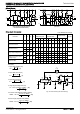
Fig. 125 Thermal resistance and derating
(b)
620mW(*15)
550mW(*16)
700mW
(
*17
)
490mW(*18)
780mW(*19)
690mW(*20)
590mW(*21)
BA2904FVM
BA2904SFV
105
870mW(*22)
660mW(*23)
610mW(*24)
(c) BA10358 family
(d) BA10324 family
POWER DISSIPATION Pd [mW]
POWER DISSIPATION Pd [mW]
POWER DISSIPATION Pd [mW]
POWER DISSIPATION Pd [mW]
A
mbient temperature
:
Ta [
℃
]
A
mbient temperature
:
Ta [
℃
]
A
mbient temperature
:
Ta [
℃
]
A
mbient temperature
:
Ta [
℃
]
BA2904SF
BA2904SFVM
85
BA2902SFV
BA2902SKN
BA2902SF
105
(e) BA2904/BA3404 family (f) BA2902 family
●Derating curves
Power dissipation(total loss) indicates the power that can be consumed by IC at Ta=25℃(normal temperature). IC is heated
when it consumed power, and the temperature of IC chip becomes higher than ambient temperature. The temperature that
can be accepted by IC chip depends on circuit configuration, manufacturing process, and consumable power is limited.
Power dissipation is determined by the temperature allowed in IC chip(maximum junction temperature) and thermal
resistance of package(heat dissipation capability). The maximum junction temperature is typically equal to the maximum
value in the storage temperature range. Heat generated by consumed power of IC radiates from the mold resin or lead
frame of the package. The parameter which indicatesthis heat dissipation capability(hardness of heat release)is called
thermal resistance, represented by the symbol θja[℃/W].The temperature of IC inside the package can be estimated by this
thermal resistance. Fig.125(a) shows the model of thermal resistance of the package. Thermal resistance θja, ambient
temperature Ta, junction temperature Tj, and power dissipation Pd can be calculated by the equation below:
θja = (Tj-Ta) / Pd [℃/W] ・・・・・ (Ⅰ)
Derating curve in Fig.125(b) indicates power that can be consumed by IC with reference to ambient temperature.Power that
can be consumed by IC begins to attenuate at certain ambient temperature. This gradient iis determined by thermal
resistance θja. Thermal resistance θja depends on chip size, power consumption, package,ambient temperature, package
condition, wind velocity, etc even when the same of package is used.
Thermal reduction curve indicates a reference value measured at a specified condition. Fig.126(c)~(f) show a derating
curve for an example of BA10358, BA10324A, BA2904S, BA2904, BA2902S, BA2902, BA3404.
(*15)
(*16) (*17) (*18) (*19) (*20) (*21) (*22) (*23) (*24) Unit
6.2 5.5 7.0 4.9 6.2 5.5 4.8 7.0 5.3 4.9 [mW/℃]
When using the unit above Ta=25[℃], subtract the value above per degree [℃].
Permissible dissipation is the value when FR4 glass epoxy board 70[mm] ×70[mm] ×1.6[mm] (cooper foil area below 3[%]) is mounted.
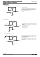
Fig. 126 Derating curve
(a)Thermal resistance
(b) Derating curve
周囲温度
Ta [
℃
]
チップ表面温度
Tj [
℃
]
消費電力 P [W]
θja = ( Tj
ー
Ta ) / Pd [
℃
/W]
Ambient temperature
Chip surface temperature
Power dissipation Pd[W]
0 50 75 100 125 15025
P1
P2
Pd (max)
LSI
の消費電力
[W]
θ' ja2
θ' ja1
Tj ' (m ax )
θja2 < θja1
周囲温度
Ta [
℃
]
θ ja2
θ ja1
Tj (m ax )
Ambient temperature
Power dissipation of LSI