
Datasheet


Technical Note
20/24
BA10393F,BA10339F,BA10339FV,BA2903SF,BA2903SFV,BA2903SFVM,BA2903F,BA2903FV,
BA2903FVM,BA2901SF,BA2901SFV,BA2901SKN,BA2901F,BA2901FV,BA2901KN,BA8391G
www.rohm.com
2010.12 - Rev.
A
© 2010 ROHM Co., Ltd. All rights reserved.
●Notes for use
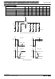
1) Unused circuits
When there are unused circuits it is recommended that they be connected as in Fig.116, setting the non-inverting input
terminal to a potential within the in-phase input voltage range (VICR).
Fig.116 Disable circuit example
2) Input terminal voltage
(BA8391 / BA2903 / BA2901 family)Applying VEE + 36V to the input terminal is possible without causing deterioration of
the electrical characteristics or destruction, irrespective of the supply voltage. However, this does not ensure normal circuit
operation. Please note that the circuit operates normally only when the input voltage is within the common mode input
voltage range of the electric characteristics.
3) Power supply (signal / dual)
The op-amp operates when the specified voltage supplied is between VCC and VEE. Therefore, the signal supply op-amp
can be used as a dual supply op-amp as well.
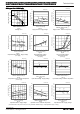
4) Power dissipation Pd
Using the unit in excess of the rated power dissipation may cause deterioration in electrical characteristics due to a rise in
chip temperature, including reduced current capability.
Therefore, please take into consideration the power dissipation (Pd) under actual operating conditions and apply a
sufficient margin in thermal design. Refer to the thermal derating curves for more information.
5) Short-circuit between pins and erroneous mounting
Incorrect mounting may damage the IC. In addition, the presence of foreign particles between the outputs, the output and
the power supply, or the output and GND may result in IC destruction.
6) Terminal short-circuits
When the output and VCC terminals are shorted, excessive output current may flow, resulting in undue heat generation
and, subsequently, destruction.
7) Operation in a strong electromagnetic field
Operation in a strong electromagnetic field may cause malfunctions.
8) Radiation
This IC is not designed to withstand radiation.
9) IC handing
Applying mechanical stress to the IC by deflecting or bending the board may cause fluctuations in the electrical
characteristics due to piezoelectric (piezo) effects.
10) Board inspection
Connecting a capacitor to a pin with low impedance may stress the IC.
Therefore, discharging the capacitor after every process is recommended. In addition, when attaching and detaching the
jig during the inspection phase, ensure that the power is turned off before inspection and removal.
Furthermore, please take measures against ESD in the assembly process as well as during transportation and storage.
Please keep this
potential in Vicm
VCC
VEE
-
+
OPEN