
User guide

Trusted
TM
RTD FTA T8841
Issue 6 Nov 07 PD-T8841 4
Table of Contents
1. Description...................................................................................................................................7
2. System Functions ........................................................................................................................8
2.1. Zero, Gain & Linearisation ...........................................................................................................8
3. Installation....................................................................................................................................8
3.1. Cable Selection............................................................................................................................8
4. Assembly Pinout Connections ...................................................................................................11
4.1. RTD1 to RTD8 ...........................................................................................................................11
4.2. IOIF ............................................................................................................................................11
4.3. PWR ..........................................................................................................................................11
5. Link Assignments.......................................................................................................................12
5.1. Two Wire Operation...................................................................................................................12
5.2. Voltage Output...........................................................................................................................12
5.3. Measurement range 0 to 100
0
C.................................................................................................13
5.4. Measurement range 0 to 300
0
C.................................................................................................13
6. Specifications.............................................................................................................................14
Figures
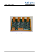
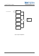
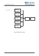
Figure 1 T8841 Layout..............................................................................................................................3
Figure 2 Single Channel Circuit ................................................................................................................7
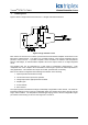
Figure 3 Typical configuration...................................................................................................................9
Figure 4 Configuration using VFTA ........................................................................................................10
Tab l e s
Table 1 RTD Connections ......................................................................................................................11
Table 2 IOIF Connections.......................................................................................................................11
Table 3 PWR Connections .....................................................................................................................11
Table 4 Two Wire Link Assignments ......................................................................................................12
Table 5 Voltage Output Link Assignments .............................................................................................12
Table 6 Range 0 to 100 deg C Link Assignments ..................................................................................13
Table 7 Range 0 to 300 deg C Link Assignments ..................................................................................13