
Manual


Trusted
TM
AI/DI FTA External Power T8834
Issue 2 Aug 06 PD-T8834 15
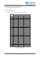
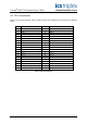
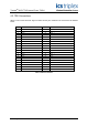
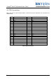
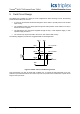
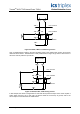
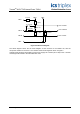
Figure 6 FTA Circuit Diagram
The above diagram shows the full circuit diagram of each channel on the T8834 FTA, with the
component numbers for channel 1. The channel circuits are arranged as shown in Figure 2.
Unused inputs should be terminated by wiring a 24V supply via a resistor (2K or 2K2) to the + terminal
and wiring the B terminal to the associated zero volts.
TB1 A
TB1 B
R13 100R
D1 7V5
CON1 VPOWER
CON1 COMMON
CON1 VSENSE
TB2 +
TB3 +
TB2 -
TB3 -
R16 4K75
R1 (Link)
R4 (Link)
R7 (unused)
R10 (Link)