
Manual
Trusted
TM
Power Supply System T82xx
Issue 9 Mar 06 PD-T82xx 9
1.3. Input Power Regulation
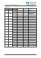
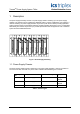
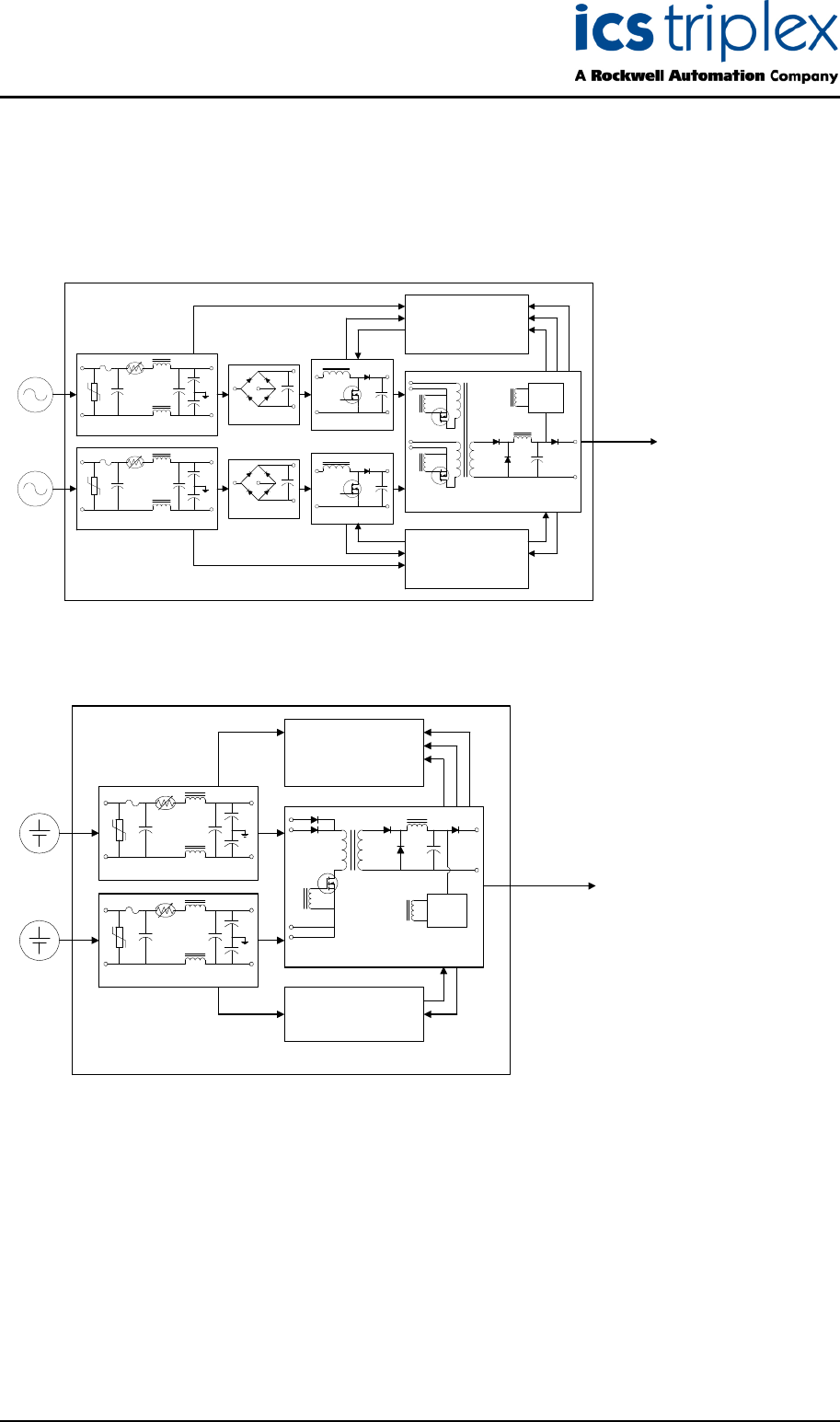
A block diagram of a typical dual ac input I/O power supply module is shown in Figure 2. A block
diagram of a typical dual dc input I/O power supply module is shown in Figure 3.
PFC
PFC
Power Supply Module
PWM
Switching Regulator
T
1:a
T
1:c
T1:b
Rectifier
Rectifier
DC
Output
I/P Filter & Protection
I/P Filter & Protection
PFC A Off
I
/P A Fail
P
FC A Fail
Source
A
Source
B
F
ail
H
igh Tempterature
R
eset
O
/P Current
Status & Control
R
emote Off
P
FC B Off
I
/P B Fail
P
FC B Fail
Status & Control
Figure 2 Block Diagram of a dual ac I/O Power Supply Module
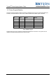
Power Supply Module
DC
Output
I/P Filter & Protection
I/P Filter & Protection
PWM
Switching Regulator
T1:a
T1:b
I/P A Fail
Fail
High Tempterature
Reset
O/P Current
Status & Control
Remote OffI/P B Fail
Status & Control
Source
A
Source
B
Figure 3 Block Diagram of a dual dc I/O Power Supply Module
Each primary power input is individually fused and filtered with both standard line filters and metal
oxide varistors (MOVs). The filters attenuate any high-frequency common mode and normal mode
noise present in the power distribution system. The MOVs clamp high-voltage transients.
Filter, rectifier, and power factor correction circuits convert primary ac input power to bulk dc voltage.
The switching regulator converts bulk dc power to regulated dc output voltage. Sensing, status, control
and timing circuits provide for the following: