
Manual


Installation/Wiring 1-35
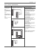
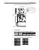
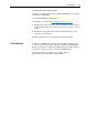
Figure 1.12 Active Converter Control Board I/O Terminal Locations
I/O Terminal Blocks
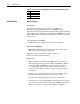
Table 1.N Active Converter Control Board I/O Terminal Block Specifications
Table 1.O Active Converter Control Board A12-P1 Terminal Descriptions
1
2
3
4
5
6
7
8
9
10
11
12
13
14
15
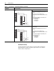
2
1
4
3
6
5
7
A12 - Active Converter
Control Assembly
A11 - Voltage Feedback
Resistor Assembly
A12 - P1
Terminals
A11 - P2
Terminals
SW1
SW1
ON
ON
DPI Slave = OFF (Default)
DPI Master = ON
Name Description
Wire Size Range
(1)
(1)
Maximum/minimum that the terminal block will accept - these are not recommendations.
Torque
Maximum Minimum Maximum Recommended
I/O Blocks Signal and power
connections
1.5 mm
2
(16 AWG)
0.14 mm
2
(28 AWG)
0.25 N-m
(2.2 lb.-in.)
0.22 N-m
(1.9 lb.-in.)
Pin Description Pin Description
1 Comm Out + 9 Aux Out N.O.
2 Comm Out - 10 Aux Out Common
3 SOC Out + 11 Analog In Signal
4 SOC Out - 12 Analog In Common
5 Comm In + 13 Safety HW Enable
6 Comm In - 14 24 Vdc
7 SOC In + 15 Aux Input
8 SOC In -