
Owner's manual
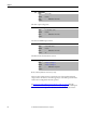
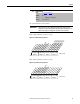
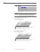
Table Of Contents
- Front Cover
- Important User Information
- Summary of Changes
- Table of Contents
- Introduction
- About the Drive
- Identifying the Drive by Cabinet Assembly ID Number
- LiquiFlo 2.0 Drive Component Locations
- Identifying the Power Module by Model Number
- AC Line I/O Board Description (Frame 3 Only)
- Standard I/O Board Description (Frame 3 Only)
- Combined I/O Board Description (Frame 4 Only)
- DPI Communication Ports
- Optional Equipment
- Planning the Installation
- Mounting The Power Module and Grounding the Drive
- Installing Input and Output Power Wiring
- Completing the Installation
- Using the Start-up Routines
- Programming Basics
- Parameter Descriptions
- Troubleshooting the Drive
- Verify that the DC Bus Capacitors are Discharged Before Servicing the Drive
- Determining Drive Status Using the Status LEDs
- About Alarms
- About Faults
- Diagnostic Parameters
- Common Symptoms and Corrective Actions
- Replacement Parts
- Board Replacement, Firmware Setup Procedures
- Troubleshooting the Drive Using the OIM
- Checking the Power Modules with Input Power Off
- Technical Specifications
- Using the OIM
- Installing and Removing the OIM
- Display Description
- OIM Menu Structure
- Powering Up and Adjusting the OIM
- Selecting a Device in the System
- Using the OIM to Program the Drive
- Monitoring the Drive Using the Process Display Screen on the OIM
- Displaying and Changing the OIM Reference
- Customizing the Process Display Screen
- Customizing the Function Keys
- Controlling the Drive From the OIM
- LiquiFlo 2.0 Drive Frame 3 Wiring Diagrams
- LiquiFlo 2.0 Drive Frame 4 Wiring Diagrams
- Index
- Back Cover
Rockwell Automation Publication D2-3518-3 - May 2013 75
Chapter 9
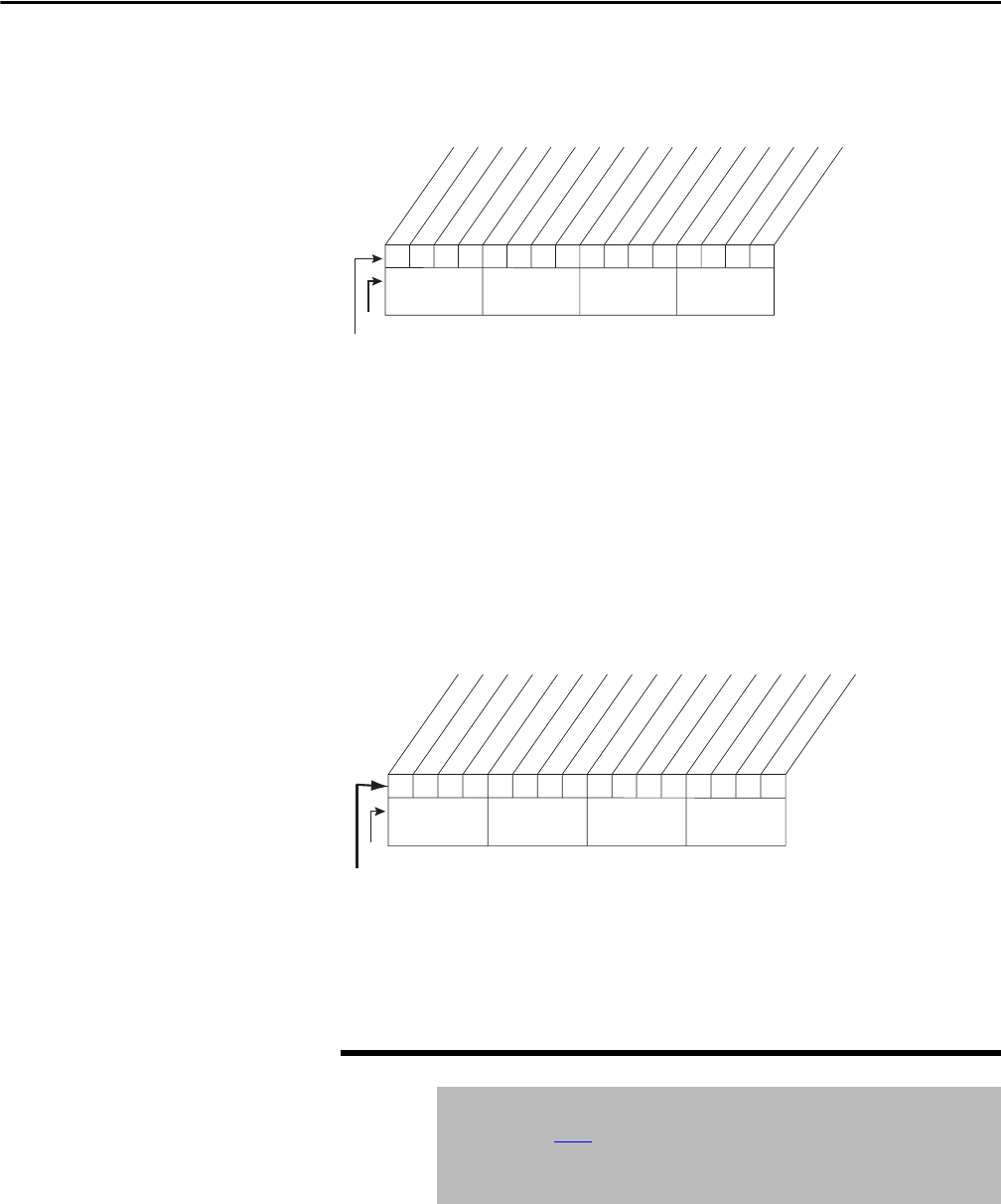
Figure 30 - Appl Digital Output (30) Frame 3
Frame 4 drives (firmware version 2.x) only:
The lower byte of this parameter controls the state of the shunt trip digital output
and the six application controlled digital outputs on the Combined I/O board.
The upper byte controls the operation of the rectifier when configured for
manual operation.
Figure 31 - Appl Digital Output (30) Frame 4
In addition to controlling digital output 3, bit 1 is also used to force the Aux Run
digital output condition to true. This only occurs if the Digital Out Sel
parameter for one of the user-configurable digital outputs is set to Aux Run.
The value entered into this parameter is output on the analog output when it is
configured for Application control. See parameter Analog Out1 Sel (342).
31 Appl Analog Out
Range: -32.767...32.767 [0.001 mA, or 0.001V (frame 4 only)]
Default: See Tabl e 6 below.
Access: 1 Path: Monitor > Application
See also: 342, 343, 344
000000xx00xxxxxx
0011234567891112131415
1=Active
0=Inactive
x =Reserved
Bit #
Factory Default Bit Values
AC Line I/O Dig. Output 1
AC Line I/O Dig. Output 2
AC Line I/O Dig. Output 3
AC Line I/O Dig. Output 4
AC Line I/O Dig. Output 5
AC Line I/O Dig. Output 6
Close Pre-charge
Enable Rectifier
Nibble 1Nibble 2Nibble 3Nibble 4
00000xxxxx
0011234567891112131415
1=Active
0=Inactive
x =Reserved
Bit #
Shunt trip
Comb. I/O Dig. Output 3
Comb. I/O Dig. Output 4
Comb. I/O Dig. Output 5
Comb. I/O Dig. Output 6
Comb. I/O Dig. Output 7
Comb. I/O Dig. Output 8
Nibble 1Nibble 2Nibble 3Nibble 4
0
0
xx
Close Pre-charge
Enable Rectifier
0
0
Powerup Default Bit Values