
Owner's manual
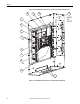
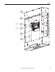
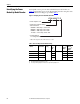
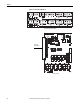
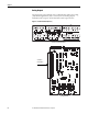
Table Of Contents
- Front Cover
- Important User Information
- Summary of Changes
- Table of Contents
- Introduction
- About the Drive
- Identifying the Drive by Cabinet Assembly ID Number
- LiquiFlo 2.0 Drive Component Locations
- Identifying the Power Module by Model Number
- AC Line I/O Board Description (Frame 3 Only)
- Standard I/O Board Description (Frame 3 Only)
- Combined I/O Board Description (Frame 4 Only)
- DPI Communication Ports
- Optional Equipment
- Planning the Installation
- Mounting The Power Module and Grounding the Drive
- Installing Input and Output Power Wiring
- Completing the Installation
- Using the Start-up Routines
- Programming Basics
- Parameter Descriptions
- Troubleshooting the Drive
- Verify that the DC Bus Capacitors are Discharged Before Servicing the Drive
- Determining Drive Status Using the Status LEDs
- About Alarms
- About Faults
- Diagnostic Parameters
- Common Symptoms and Corrective Actions
- Replacement Parts
- Board Replacement, Firmware Setup Procedures
- Troubleshooting the Drive Using the OIM
- Checking the Power Modules with Input Power Off
- Technical Specifications
- Using the OIM
- Installing and Removing the OIM
- Display Description
- OIM Menu Structure
- Powering Up and Adjusting the OIM
- Selecting a Device in the System
- Using the OIM to Program the Drive
- Monitoring the Drive Using the Process Display Screen on the OIM
- Displaying and Changing the OIM Reference
- Customizing the Process Display Screen
- Customizing the Function Keys
- Controlling the Drive From the OIM
- LiquiFlo 2.0 Drive Frame 3 Wiring Diagrams
- LiquiFlo 2.0 Drive Frame 4 Wiring Diagrams
- Index
- Back Cover
Rockwell Automation Publication D2-3518-3 - May 2013 29
Chapter 2
Combined I/O Board
Description (Frame 4 Only)
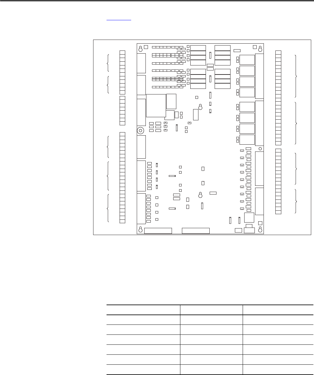
Figure 11 shows terminal block locations on the Combined I/O Board.
Figure 11 - Combined I/O Board (Frame 4)
Digital Inputs
The combined I/O board provides hardware for six user-configurable digital
inputs, using connector positions designated DI3...DI8. The following table
shows the correspondence between the digital input and the inverter parameter
used to configure it.
The states of all six user-configurable digital inputs are visible in inverter
parameter Dig In Status (216).
The digital inputs that use connector positions DI1 and DI2 on the combined
I/O board are not user-configurable. The status of these two digital inputs are
visible in rectifier parameter Dig In Status (216).
5
1
2
3
4
5
1
7
6
TB4
3
2
4
7
6
8
9
TB3
1
2
6
3
4
5
6
7
8
9
10
2
11
12
TB2
1
4
3
5
10
8
7
9
12
11
TB1
DI 6
DI 24V-
DI COM 2
DI 8
DI 7
DI 2
DI 24V-
DI 24V+
DI 5
DI 4
DI COM 1
DI 3
DI 24V+
DI 1
GATEKILL -
GATEKILL +
DIGITAL
OUTPUT
2
DO 8 NO
DO 8 COM
DO 3 NC
DO 8 NC
DO 7 NO
DO 7 COM
DO 7 NC
DO 6 NO
DO 6 COM
DO 6 NC
DO 5 NO
DIGITAL
OUTPUT
1
DO 4 COM
DO 5 COM
DO 5 NC
DO 4 NO
DO 3 NO
DO 4 NC
DO 3 COM
DO 1 NO
DO 2 COM
DO 2 NO
DO 2 NC
DO 1 NC
DO 1 COM
DIGITAL
INPUT
2
DIGITAL
INPUT
1
+12V 1
AO 1-
OUTPUT
ANALOG
AO 3- 6
AO 4- 8
AO 4+ 7
AO 2-
AO 3+ 5
4
AO 2+ 3
2
INPUT
ANALOG
ENCODER
INPUT
TB9
AO 1+ 1
AI 4-
AI 4+
8
7
AI 3-
AI 3+
6
5
AI 2-
AI 2+
4
3
B+
TB8
AI 1+
AI 1- 2
1
B- 6
A+ 3
A-
5
4
COMMON
2
G1 1
TEMPSW RCT
TEMPSW INV
VOLTAGE
GRID
SHUNT TRIP 3
PRECHARGE FB 7
TB10
5
6
SW 24V 4
G3 5
TB7
CNTRL PWR
PRECHARGE OUT 2
1
G2 3
VOLTAGE
LINE
L2 3
TB6
L3 5
TB5
L1 1
Inverter Parameter Number Inverter Parameter Name Connector Position Designator
361 Digital In1 Sel DI3
362 Digital In2 Sel DI4
363 Digital In3 Sel D15
364 Digital In4 Sel DI6
365 Digital In5 Sel DI7
366 Digital In6 Sel DI8