
Owner's manual
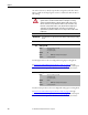
Table Of Contents
- Front Cover
- Important User Information
- Summary of Changes
- Table of Contents
- Introduction
- About the Drive
- Identifying the Drive by Cabinet Assembly ID Number
- LiquiFlo 2.0 Drive Component Locations
- Identifying the Power Module by Model Number
- AC Line I/O Board Description (Frame 3 Only)
- Standard I/O Board Description (Frame 3 Only)
- Combined I/O Board Description (Frame 4 Only)
- DPI Communication Ports
- Optional Equipment
- Planning the Installation
- Mounting The Power Module and Grounding the Drive
- Installing Input and Output Power Wiring
- Completing the Installation
- Using the Start-up Routines
- Programming Basics
- Parameter Descriptions
- Troubleshooting the Drive
- Verify that the DC Bus Capacitors are Discharged Before Servicing the Drive
- Determining Drive Status Using the Status LEDs
- About Alarms
- About Faults
- Diagnostic Parameters
- Common Symptoms and Corrective Actions
- Replacement Parts
- Board Replacement, Firmware Setup Procedures
- Troubleshooting the Drive Using the OIM
- Checking the Power Modules with Input Power Off
- Technical Specifications
- Using the OIM
- Installing and Removing the OIM
- Display Description
- OIM Menu Structure
- Powering Up and Adjusting the OIM
- Selecting a Device in the System
- Using the OIM to Program the Drive
- Monitoring the Drive Using the Process Display Screen on the OIM
- Displaying and Changing the OIM Reference
- Customizing the Process Display Screen
- Customizing the Function Keys
- Controlling the Drive From the OIM
- LiquiFlo 2.0 Drive Frame 3 Wiring Diagrams
- LiquiFlo 2.0 Drive Frame 4 Wiring Diagrams
- Index
- Back Cover

144 Rockwell Automation Publication D2-3518-3 - May 2013
Chapter 9
One of the selections (1=Fault) stops the drive on signal loss. All other choices
make it possible for the input signal to return to a usable level while the drive is
still running.
Sets the highest value to the user-configurable analog input 2 scaling block.
See AC Line I/O Board Description (Frame 3 Only)
on page 25 through
Combined I/O Board Description (Frame 4 Only)
on page 29 for a description
of I/O hardware that is present on this drive and is controlled by the inverter.
Sets the lowest input value to the user-configurable analog input 2 scaling block.
See AC Line I/O Board Description (Frame 3 Only)
on page 25 through
Combined I/O Board Description (Frame 4 Only)
on page 29 for a description
of I/O hardware that is present on this drive and is controlled by the inverter.
ATTENTION: Setting parameter 324 to a value greater than 1 allows the input
signal to return to a usable level while the drive is running. If a lost analog
signal is restored while the drive is running, the drive ramps to the restored
reference level at the rate specified in Accel Time 1 (140), Accel Time 2 (141),
Decel Time 1 (142), and Decel Time 2 (143). Be aware that an abrupt speed
change may occur depending upon the new reference level and the rate
specified in these parameters. Failure to observe this precaution could result in
bodily injury.
IMPORTANT
Note that there is no signal loss detection while the input is in bipolar voltage
mode.
325 Analog In 2 Hi
Range: 4.000...20.000 mA [0.001 mA]
-/+10.000V [0.1V]
0.0...10.000V [0.1V]
Default: 10V
Access: 0 Path: Inputs & Outputs > Analog Inputs
See also: 91, 92, 320, 326, 327
326 Analog In 2 Lo
Range: 4.000...20.000 mA [0.001 mA]
-/+10.000V [0.1V]
0.0...10.000V [0.1V]
Default: 0.000V
Access: 0 Path: Inputs & Outputs > Analog Inputs
See also: 91, 92, 320, 326, 327