
Owner's manual
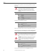
Table Of Contents
- Front Cover
- Important User Information
- Summary of Changes
- Table of Contents
- Introduction
- About the Drive
- Identifying the Drive by Cabinet Assembly ID Number
- LiquiFlo 2.0 Drive Component Locations
- Identifying the Power Module by Model Number
- AC Line I/O Board Description (Frame 3 Only)
- Standard I/O Board Description (Frame 3 Only)
- Combined I/O Board Description (Frame 4 Only)
- DPI Communication Ports
- Optional Equipment
- Planning the Installation
- Mounting The Power Module and Grounding the Drive
- Installing Input and Output Power Wiring
- Completing the Installation
- Using the Start-up Routines
- Programming Basics
- Parameter Descriptions
- Troubleshooting the Drive
- Verify that the DC Bus Capacitors are Discharged Before Servicing the Drive
- Determining Drive Status Using the Status LEDs
- About Alarms
- About Faults
- Diagnostic Parameters
- Common Symptoms and Corrective Actions
- Replacement Parts
- Board Replacement, Firmware Setup Procedures
- Troubleshooting the Drive Using the OIM
- Checking the Power Modules with Input Power Off
- Technical Specifications
- Using the OIM
- Installing and Removing the OIM
- Display Description
- OIM Menu Structure
- Powering Up and Adjusting the OIM
- Selecting a Device in the System
- Using the OIM to Program the Drive
- Monitoring the Drive Using the Process Display Screen on the OIM
- Displaying and Changing the OIM Reference
- Customizing the Process Display Screen
- Customizing the Function Keys
- Controlling the Drive From the OIM
- LiquiFlo 2.0 Drive Frame 3 Wiring Diagrams
- LiquiFlo 2.0 Drive Frame 4 Wiring Diagrams
- Index
- Back Cover
108 Rockwell Automation Publication D2-3518-3 - May 2013
Chapter 9
For the LiquiFlo 2.0 drive, always set this parameter to 0 (Disabled).
Selects whether the internal or an external DB resistor is used.
Proportional gain for the bus regulator. Used to adjust regulator response.
ATTENTION: The adjust freq portion of the bus regulator function is extremely
useful for preventing nuisance overvoltage faults resulting from aggressive
decelerations, overhauling loads, and eccentric loads. It forces the output
frequency to be greater than commanded frequency while the drive’s bus
voltage is increasing towards levels that would otherwise cause a fault.
However, it can also cause either of the following two conditions to occur:
• Fast positive changes in input voltage (more than a 10% increase within
6 minutes) can cause uncommanded positive speed changes; however, an
OverSpeed Limit fault occurs if the speed reaches Max Speed + Overspeed
Limit. If this condition is unacceptable, action should be taken to 1) limit supply
voltages within the specification of the drive, and 2) limit fast positive input
voltage changes to less than 10%. Without taking such actions, if this
operation is unacceptable, the adjust freq portion of the bus regulator function
must be disabled (see parameters 161 and 162).
• Actual deceleration times can be longer than commanded deceleration times;
however, a Decel Inhibit fault is generated if the drive stops decelerating
altogether. If this condition is unacceptable, the adjust freq portion of the bus
regulator must be disabled (see parameters 161 and 162). In addition,
installing a properly sized dynamic brake resistor provides equal or better
performance in most cases.
Note that these faults are not instantaneous and have shown test results that take
between 2 and 12 seconds to occur.
163 DB Resistor Type
Range: 0 = Internal Res
1 = External Res
2 = None
Default: 2 = None
Access: 0 Path: Dynamic Control > Stop/Brake Modes
See also: 161, 162
164 Bus Reg Kp
Range: 0...10000
Default: 1200
Access: 1 Path: Dynamic Control > Stop/Brake Modes
See also: