
User Manual

Parameter-to-Register Cross Reference
B-1
APPENDIX B
Parameter-to-Register
Cross Reference
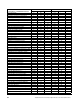
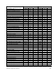
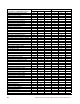
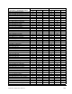
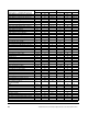
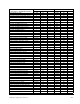
Description or GV3000/SE Parameter
Read Only Read/Write
Drop Register Bit Drop Register Bit
AC Line Volts (H.021) 3, V/Hz 21 3, V/Hz 53
AC Line Volts (U.018) 3, Vector 14 3, Vector 43
Accel Time 1 (RAMP 1) (P.001) 1 17 1 37
Analog input signal loss (AIn) 1 13 13 n/a
Asymmetrical bus charge (UbS) 1 13 8 n/a
Auto or manual reference selected 1 26 1 n/a
AUTO/MAN Key Disable (P.052) 2 24 3 2 38 3
Avoidance Frequency Band 1 (H.011) 3, V/Hz 11 3, V/Hz 43
Avoidance Frequency Band 2 (H.013) 3, V/Hz 13 3, V/Hz 45
Avoidance Frequency Band 3 (H.015) 3, V/Hz 15 3, V/Hz 47
Avoidance Frequency Enable (H.009) 3, V/Hz 9 0 3, V/Hz 41 0
Avoidance Frequency Midpoint 1 (H.010) 3, V/Hz 10 3, V/Hz 42
Avoidance Frequency Midpoint 2 (H.012) 3, V/Hz 12 3, V/Hz 44
Avoidance Frequency Midpoint 3 (H.014) 3, V/Hz 14 3, V/Hz 46
bYC 1 13 1 n/a
Carrier Frequency (kHz) (P.047) 2 26 2 47
CHS 1 12 9 n/a
Clear error log n/a 1 32 8
Communication loss between
Regulator/PC/OIM (SrL)
11210n/a
Configurable Booleans (read) 2 19 n/a
Control Source (P.000) 1 16 n/a
Control word n/a 1 53
Country Defaults (P.049) 2 28 2 49
Current Compounding Gain (U.026) 2 25 3, Vector 49
Current Limit (P.005) 1 21 1 41
DC Braking Current (H.007) 3, V/Hz 7 3, V/Hz 39
DC Braking Enable (H.005) 3, V/Hz 5 0 3, V/Hz 37 0
DC Braking Start Frequency (H.006) 3, V/Hz 6 3, V/Hz 38
DC Braking Time (H.008) 3, V/Hz 8 3, V/Hz 40
DC bus charging bypass contactor (bYC) 1 13 1 n/a
Decel Time (RAMP 1) (P.002) 1 18 1 38
Default parameter restore (CHS) 1 12 9 n/a
Diagnostics Display (P.091) n/a n/a
Diagnostics Source (P.090) n/a n/a
Draw Gain Percentage (P.016) 1 23 1 46
Drive fault latch bits (word 1) 1 12 n/a
Drive fault latch bits (word 2) 1 13 n/a
Drive overtemperature (OH) 1 12 7 n/a