
Manual

Installation Instructions
Bulletin 842-SPA Serial to Parallel Adaptor
IMPORTANT: SAVE THESE INSTRUCTIONS FOR FUTURE USE.
Specifications
Size 103 x 165mm (4 x 6.5in)
Voltage Supply 11-32V DC
Supply Current 250mA (without load)
Operating Temperature
0_C to 50_C (32_F to 122_F)
Output Driver (parallel) PushĆpull, 10-32V, 35mA (max)
Input (SSI) RS422
Maximum SSI Cable Length 350m @ 125kHz; 25m @ 500kHz
Mounting Instructions
1. Locate and mount the 842–CH cardholder (purchased
separately) close to the controller. See the Dimensions
section to determine the 842–CH card holder hole
locations.
2. Wire the connections according to the a) Electrical
Connections b) Jumpers Needed and c) Direction Control
sections using wire size 26–16 AWG.
IMPORTANT: Wiring must be in accordance with the
National Electric Code and applicable local
codes and ordinances.
3. Insert the 842–SPA into the cardholder. Set the Hex
Function switch on the 842–SPA to the appropriate setting
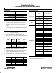
as shown in Table 1 below:
Switch
Setting
Clock
Frequency
SSI
Input
Parallel
Output
4 500kHz Binary Binary
4 500kHz Gray Gray
5 125kHz Binary Binary
5 125kHz Gray Gray
6 500kHz Gray Binary
7 125kHz Gray Binary
4. Apply power supply of 11–32V DC to the 842–SPA.
5. The 842–SPA begins sending clock pulses and receives
data pulses in the synchronous serial interface (SSI)
format. An example timing diagram is in the Timing
Diagrams section.
6. The parallel output data can be found on the following bits
according to Table 2 below:
842A Encoder
Type
Pulses
Per Rev.
Bits Used
LSB-MSB
No. of
Revs.
Bits Used
LSB-MSB
A 8192 1-13 2048 14-24
B 4096 1-12 4096 13-24
C 2048 1-11 8192 12-24
D 4096 1-12 512 13-21
E 4096 1-12 256 13-20
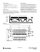
Electrical Connections
Type Function 842-CH Terminal
842-SPA and Output Driver
Ground
1A, 2C, 25AÊ
842-SPA Power
32C,13CÊ
Power & Ground
Parallel Output Driver
Power
31A
Encoder Power 32A
Encoder Ground
1C,25CÊ
Data + 26C
SSI
Data - 26A
SSI
Clock + 27C
Clock - 27A
Error Bit
2AË
Error Bit
2AË
Bit 1 3C
Bit 2 3A
Bit 3 4C
Bit 4 4A
Bit 5 5C
Bit 6 5A
Bit 7 6C
Bit 8 6A
Bit 9 7C
Bit 10 7A
Parallel Output
STbl2f
Bit 11 8C
p
See Table 2 for
Bit Distri
b
uti
o
n
Bit 12 8A
Bit
Distribution
Bit 13 9C
Bit 14 9A
Bit 15 14C
Bit 16 14A
Bit 17 15C
Bit 18 15A
Bit 19 16C
Bit 20 16A
Bit 21 17C
Bit 22 17A
Bit 23 18C
Bit 24 18A
Ê Terminals are connected internally on the 842-SPA.
Ë The Error Bit is normally logic 0. If there is a power interruption (i. e. - low voltage)
during data transmission, the Error Bit is set to logic 1.