
Manual

6-86 Component Definition and Maintenance
7000-UM150I-EN-P – June 2013 7000 “B” Frame
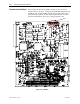
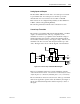
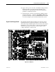
CIB
J4A
Process Loop Receiver
Shielded Twisted Pair
SHLD
1
2
3
4
Ia
CIB
J4A
Process Loop Receiver
Shielded Twisted Pair
SHLD
1
2
3
4
Ia
Figure 6.62 – Recommended Connection to CIB Transmitter
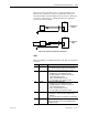
Current Loop Receiver
The receiver can accept either 0-20mA or 4-20mA inputs from an
external transmitter. The transmitter must have a minimum loop
compliance of 5V to satisfy the input impedance of 250 ohms.
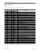
A block diagram of the receiver is shown below.
DSP
FPGA
Isolated
DC/DC
Converter
A/D
Isolation
Amplifier
250R
3
4
1
2
+15V @ 2W
Buffer
J4B
x
1
u
1
DSP
FPGA
Isolated
DC/DC
Converter
A/D
Isolation
Amplifier
250R
3
4
1
2
+15V @ 2W
Buffer
J4B
x
1
u
1
Figure 6.63 – Process Loop Receiver Block Diagram
Customer Interface Board
(cont.)