! # # " $" ! " $ " "$ # # % # $# # DANGER ONLY QUALIFIED ELECTRICAL PERSONNEL FAMILIAR WITH THE CONSTRUCTION AND OPERATION OF THIS EQUIPMENT AND THE HAZARDS INVOLVED SHOULD INSTALL, ADJUST, OPERATE, AND/OR SERVICE THIS EQUIPMENT. READ AND UNDERSTAND THIS MANUAL IN ITS ENTIRETY BEFORE PROCEEDING. FAILURE TO OBSERVE THIS PRECAUTION COULD RESULT IN SEVERE BODILY INJURY OR LOSS OF LIFE.
Table of Contents 1.0 Introduction . . . . . . . . . . . . . . . . . . . . . . . . . . . . . . . . . . . . . . . . . . . . . . . 1Ć1 1.1 Related Publications . . . . . . . . . . . . . . . . . . . . . . . . . . . . . . . . . . . . . 1Ć1 1.2 Related Hardware and Software . . . . . . . . . . . . . . . . . . . . . . . . . . . 1Ć2 2.0 Mechanical/Electrical Description . . . . . . . . . . . . . . . . . . . . . . . . . . . 2Ć1 2.1 Mechanical Description . . . . . . . . . . . . . . . . . . . . . . . . . . . . .
Appendices Appendix A Technical Specifications . . . . . . . . . . . . . . . . . . . . . . . . . . . . . . . . . . . . . . AĆ1 Appendix B Module Block Diagram . . . . . . . . . . . . . . . . . . . . . . . . . . . . . . . . . . . . . . BĆ1 Appendix C Field Connections . . . . . . . . . . . . . . . . . . . . . . . . . . . . . . . . . . . . . . . . . . . CĆ1 Appendix D Related Components . . . . . . . . . . . . . . . . . . . . . . . . . . . . . . . . . . . . . . . . DĆ1 Appendix E Configuration Task . . . . .
Figure 1.1 Ć Voltage Input Module Hardware Configuration . . . . . . . . . . . . 1Ć2 Figure 2.1 Figure 2.2 Ć Module Faceplate . . . . . . . . . . . . . . . . . . . . . . . . . . . . . . . . . . . . . 2Ć2 Ć Typical Voltage Input Channel . . . . . . . . . . . . . . . . . . . . . . . . . . 2Ć4 Figure 3.1 Figure 3.2 Figure 3.3 Ć Terminal Board Assembly Mounting Dimensions . . . . . . . . . . 3Ć2 Ć Voltage Input Module Connections . . . . . . . . . . . . . . . . . . . . . .
fafadfdfdasfdsfdsdsdfdsfdsfdsfsdfdsa afdfdsfdsfdfdsfdsfsadfda asfdfaddfdd
1.0 INTRODUCTION The products described in this manual are manufactured and/or distributed by Reliance Electric Industrial Company. The Multibus Ćcompatible Voltage Analog Input module (M/N 61C542A) allows you to connect up to 16 singleĆended or eight differential +10V input signals to AutoMate , AutoMax , and DCS 5000 systems. The voltage input signals may be generated from process control sensors, transmitters, transducers, or drive controllers.
IEEE 518 GUIDE FOR THE INSTALLATION OF ELECTRICAL EQUIPMENT TO MINIMIZE ELECTRICAL NOISE INPUTS TO CONTROLLERS FROM EXTERNAL SOURCES 1.2 Related Hardware and Software The Voltage Input module, M/N 61C542, contains the following: 1. One Voltage Input module The following items must be purchased separately: Panel mount terminal board and cable assembly, M/N 61C547. One is required per module. or DIN rail mount terminal board and cable assembly, M/N 61C548. One is required per module.
2.0 MECHANICAL/ELECTRICAL DESCRIPTION The following is a description of the faceplate LED, field termination connectors, and electrical characteristics of the field connections. 2.1 Mechanical Description The Voltage Input module is a MultibusĆcompatible printed circuit board assembly that plugs into the backplane of the DCS 5000/AutoMax or AutoMate rack. It consists of a printed circuit board, a faceplate, and a protective enclosure.
% $" % $ ! # %
2.2 Electrical Description The module provides analog voltage information to AutoMax and AutoMate systems. The module has sixteen singleĆended channels which can alternately be configured as eight differential channels. SingleĆended operation versus differential operation is programmable on a perĆchannelĆpair basis via register 31. Differential channel pairing is hardwareĆdefined as follows: channels 0Ć1, 2Ć3 ... 14Ć15, with the evenĆnumber channel being the plus or high input.
modules can read all locations within the module's slot address, but can only write to registers 23 through 31. The module performs a full complement of powerĆup diagnostics which must execute successfully before the module enters the run mode. Any diagnostic test failure results in a module shutdown. Terminal Board and Cable Assembly (M/N 61C547/61C548) 220K A UserĆSupplied Voltage Transmitter (SingleĆ Ended) VIN+ Analog Common 1A 10m +15V 220K 2A 3B 3A 0.1 F M U X 0.
3.0 INSTALLATION This section describes how to install and remove the module and its cable assemblies. DANGER ONLY QUALIFIED ELECTRICAL PERSONNEL FAMILIAR WITH THE CONSTRUCTION AND OPERATION OF THIS EQUIPMENT AND THE HAZARDS INVOLVED SHOULD INSTALL, ADJUST, OPERATE, AND/OR SERVICE THIS EQUIPMENT. READ AND UNDERSTAND THIS MANUAL IN ITS ENTIRETY BEFORE PROCEEDING. FAILURE TO OBSERVE THIS PRECAUTION COULD RESULT IN SEVERE BODILY INJURY OR LOSS OF LIFE.
PANELĆMOUNT TERMINAL BOARD M/N 61C547 Hole Size: 0.27" x 0.20" Oval 0.68 cm x 0.50 cm Hole Center Line Spacing 7.65" 6.70" 19.4 cm 17.0 cm 7.17" 18.2 cm 3.43" 8.7 cm Depth: 2.07" 5.2 cm DIN RAILĆMOUNT TERMINAL BOARD M/N 61C548 6.70" 17.0 cm 2.77" 7.0 cm Depth DIN TSĆ32 : 2.77 Rail Mounted 7.0 cm Figure 3.
Cable and Terminal Board Assembly Field Wiring (Belden 9501) (M/N 61C547 or M/N 61C548) 2 Wires + Shield Transmitter 0 Transmitter 1 2 Wires + Shield Transmitter 15 2 Wires + Shield AutoMax or AutoMate Multibus Rack Voltage Input Module 12 AWG Green Wire Chassis Common for Cable Shields Figure 3.2 Ć Voltage Input Module Connections Step 3. Fasten the wires from the transmitters to the screwĆtype connectors on the terminal board assemblies.
Step 8. Connect the programming terminal to the system and run the ReSource Programming Executive Software. Stop all programs that may be running. Configure the voltage input channels you are using by following the procedure in section 4.2. You cannot monitor the registers on the module until you have configured the channels. When you are done configuring, read the channels' default values to verify that the installation is correct. Refer to sections 4.1.1 to 4.1.17 for the default values.
3.3 Module Replacement Use the following procedure to replace a module: Step 1. Turn off power to the rack and all external devices. DANGER THIS EQUIPMENT IS AT LINE VOLTAGE WHEN AĆC POWER IS CONNECTED. DISCONNECT AND LOCK OUT ALL UNGROUNDED CONDUCTORS OF THE AĆC POWER LINE. FAILURE TO OBSERVE THESE PRECAUTIONS COULD RESULT IN SEVERE BODILY INJURY OR LOSS OF LIFE. Step 2. Use a screwdriver to loosen the screws holding the DĆshell connector to the module. Remove the DĆshell connector. Step 3.
fafadfdfdasfdsfdsdsdfdsfdsfdsfsdfdsa afdfdsfdsfdfdsfdsfsadfda asfdfaddfdd
4.0 PROGRAMMING This section describes how the data is organized in the module and provides examples of how the module is accessed by application programs. For DCS 5000 and AutoMax version 2.1 and earlier, you must assign variable names to registers by writing a configuration task. For AutoMax version 3.0 and later, you define registers using the ReSource AutoMax Programming Executive.
Table 4.
Table 4.
4.1.1 A/D Data Registers (Registers 0 to 15) Registers 0 to 15 hold the latest numeric data from configured analog voltage input channels 0 to 15. This data has been filtered (50 or 60 Hz filters) and, if the cycle averaging option has been enabled, averaged together. See figure 4.1. The data is in a 15Ćbit plus a signĆbit integer format. The data is displayed in engineering units specified by the Maximum Scaling Value (register 24) and Minimum Scaling Value (register 25).
4.1.3 High Alarm Status Register (Register 17) Register 17 indicates the current status of each configured channel's High alarm. See figure 4.3. A bit is set in this register whenever a channel's input value exceeds the configured High alarm limit. The bit is reset when the input value returns to a level below the configured limit. When two channels are configured as a differential pair, only the bit representing the first channel (evenĆnumber) will be updated.
4.1.5 Low Low Alarm Status Register (Register 19) Register 19 indicates the current status of each configured channel's Low Low alarm. See figure 4.5. A bit is set in this register whenever a channel's input value is less than the configured Low Low alarm limit. The bit is reset when the input value returns to a level above the configured limit. When two channels are configured as a differential pair, only the bit representing the first channel (evenĆnumber) will be updated.
4.1.7 Channel Configuration Status Register (Register 21) Register 21 indicates whether or not a channel has been configured. See figure 4.7. A bit is set in this register when a channel receives a correct write configuration command. Note that if two channels are configured as a differential pair, both channel status bits will be set. The bit remains set until it is cleared by a reset configuration command from register 31.
Bit 15 will remain set after a configuration command is received until bits 12 to 15 of the Configuration Command Register (register 31) are reset to zero. When bits 12 to 15 of register 31 are reset to zero, the Voltage Input module resets bit 15 of register 22, which allows you to enter another configuration command. If you try to enter another configuration command before bit 15 of register 22 is reset, error bits 7 and 14 in register 22 will be set. 4.1.
If the register contains a value of zero or one, no input data will be averaged together. If the register contains a negative number or a number greater than 60, a configuration error will result in register 22. As the number of input samples increases, the time span of averaging increases, which results in a less current input value for use in the application program. See figure 4.9 for an equation to determine the amount of time needed to calculate an average input value for registers 0 to 15.
4.1.15 Low Alarm Register (Register 29) Register 29 defines the Low alarm limit. If a channel's input value is less than this limit, the channel's corresponding bit in register 18 is set to one. The value in register 29 is a 15Ćbit plus a signĆbit integer. This value must be in engineering units if scaling is used. If scaling is used, this value must be smaller than the Maximum Scaling Value (register 24) and equal to or larger than the Minimum Scaling Value (register 25).
Bits 0Ć15 15 14 13 12 11 10 RW RW RW RW - 5 4 3 - RW RW RW RW - 9 8 7 6 - - 2 1 0 - RW RW Bits 1 and 0 = When An Input Value Is Out Of Range, The Voltage Input Module Will: 0ă0ă=ăRetain Old Input Value 0ă1ă=ăForce Input Value to Low Low Alarm Value 1ă0ă=ăForce Input Value to High High Alarm Value 1ă1ă=ăRetain Old Input Value Bits 5 to 2 = Reserved Bit 6=ĂCycle Frequency Averaging ąă 0=ĂEnable ąă 1=ĂDisable Bit 7=ĂSquare Root Extraction ą 0=ĂDisable ąă 1=ĂEnable Bit 8 = Differential
Bit 7 defines whether or not square root extraction is enabled for the channel specified in register 23. The default condition (0) disables square root extraction. When square root extraction is enabled, you must be in unipolar mode. The square root function provides flow information directly from a differential pressure input. If the specified channel has square root extraction enabled and does not use engineering units, the flow information provided is in the range of 0 to +4095.
4.2 Analog Input Channel Configuration Procedure Analog input channel configuration information is stored onĆboard the Voltage Input module. At system powerĆup, default values are automatically placed in the module's memory. You can change these default values on a channelĆbyĆchannel basis. See figure 4.11 and the steps that follow.
VOLTAGE INPUT MODULE POWERĆUP SET BITS 12 TO 15 OF REGISTER 31 =0 BIT 15 OF REG 22 = 0? NO WAIT YES ENTER CONFIG. INFORMATION IN REGS. 23Ć30 ENTER DESIRED COMMAND OPTIONS IN REG. 31 BIT 15 OF REG 22 = 1? NO WAIT YES BIT 14 OF REG 22 = 1? NO YES CHECK CONTENTS OF REG 22 FOR ERROR CODE Figure 4.
Use the following procedure to configure a channel: Step 1. Set bits 12 to 15 of register 31 equal to zero. This resets bit 15 of register 22 and places the module in the READY state. When the READY state is enabled, the module is ready to process a configuration command. Monitor bit 15 until it is equal to zero before continuing with Step 2. Step 2. Select the channel to be configured by writing the appropriate number to the Channel Number Register (Register 23).
4.3 Monitoring Data and Configuration Register Values Run the ReSource Programming Executive Software. Use the MONITOR function in DCS 5000/ AutoMax systems or the POINT MONITOR function in AutoMate systems to check the contents of the registers. Note that you need to configure the channels before you can monitor their contents. Status register values are in hexadecimal format. All other register values are in decimal. 4.
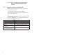
Channel 2: Operating Pressure Process Parameters Configuration Values Maximum = 1960 psig Reg. 24 = 10000 (Scaled in 0.01% of span) Minimum = 1940 psig Reg. 25 = 0 High High Alarm = 1958 psig Reg. 27 = 9000 High Alarm = 1955 psig Reg. 28 = 7500 Low Alarm = 1945 psig Reg. 29 = 2500 Low Low Alarm = 1942 psig Reg. 30 = 1000 If you are using AutoMax version 2.1 or earlier, you will need to define common (systemĆwide) variables in a configuration task before writing an application task.
10 20 30 40 45 50 55 60 65 70 75 80 90 100 110 120 130 200 210 220 230 240 245 300 310 320 330 340 400 410 420 430 440 500 510 520 530 540 600 610 620 630 640 650 660 670 680 690 700 710 720 730 ! ! ! This task configures three channels: ! Channel 0 monitors the level of a liquid in a tank ! Channel 1 monitors the startup pressure of a process ! Channel 2 monitors the operating pressure of a process ! If any configuration fails, SHUTDOWN@ is set ! ! This task checks for alarms once per second.
990 1000 1010 1020 ! ! ******************** INITIALIZATION ********************** ! ! Configure the first three channels using the data ! statements at 8000.
4.5 Sample AutoMate Voltage Input Application Program The sample AutoMate voltage input application program in figure 4.13 is written for a Voltage Input module in a remote rack that is controlled by an AutoMate 40 processor. If your system uses an AutoMate 30 processor, the addresses you use must be changed accordingly. If the Voltage Input module were in a local rack, LOCIN/LOCOUT commands would replace the REMIN/REMOUT commands.
The sample program uses the following memory locations: Bit 00.00 = Bit to be set by the user when a channel is to be configured. Bit 1700.00 = Bit used to detect the rising edge of Bit 00.00.
Register 3005= Register contains the voltage input channel's High High alarm value. This value is provided by the data table in the 5000Ćseries registers. Register 3006= Register contains the voltage input channel's High alarm value. This value is provided by the data table in the 5000Ćseries registers. Register 3007= Register contains the voltage input channel's Low alarm value. This value is provided by the data table in the 5000Ćseries registers.
Sequence 1: Test if write configuration is enabled 0 .00 [ą] Sequence 2: 1700 .00 [ą] Sequence 3: 1700 .00 [ą] Sequence 4: 1610 .00 [ą] 1700 .00 (ą) On rise of the write configuration bit, enter State 0 EN EN 1600 .00 (ą) MOVK LENGTH: 1 VALUE: 0000 0000 0000 0001 DEST: 1610 On rise of the write configuration bit, POINTER and CHANNEL = 0 EN MOVK LENGTH: 2 VALUE: 0 DEST: 3000 EN 1600 .01 (ą) State 0 = Write the READY command to the Voltage ăąąąąĂInput module (register 31, octal 37) 1600 .
Sequence 5: 1610 .00 [ą] State 0 = Read the configuration status from the ąąąąĂăVoltage Input module (register 22, octal 26) EN REMIN EN LENGTH: 1 SLOT: DROP: RSLOT: CHAN: DEST: VALUE: 1600 .03 (ą) 1776 .00 (ą) 6 1 2 26 1611 Sequence 6: 1610 .00 [ą] State 0 = If the configuration complete bit = 0, ąąąąăĂthen advance to State 1 1611 1600 .17 .04 EN EN [Ă/Ă] (ą) MOVK LENGTH: 1 VALUE: 0000 0000 0000 0010 DEST: 1610 Sequence 7: 1610 .
Sequence 8: 1610 .01 [ą] State 1 = Write configuration data to the Voltage Input module (starting from register 23, (octal 27), with a length of 9) EN REMOUT EN LENGTH: 9 SRC: VALUE: SLOT: DROP: RSLOT: CHAN: Sequence 9: 1610 .01 [ą] 1600 .06 (ą) 1776 .00 (ą) 3001 6 1 2 27 State 1 = Read the configuration status from the Voltage Input module (register 22, octal 26) EN REMIN EN LENGTH: 1 SLOT: DROP: RSLOT: CHAN: DEST: VALUE: 6 1 2 26 1611 1600 .07 (ą) 1776 .
Sequence 11: State 1 = If the configuration is complete and there ąąąąăĂis no error, advance to State 2 1610 1611 1611 .01 .17 .16 [ą] [ą] [Ă/Ă] EN MOVK EN 1600 .11 (ą) LENGTH: 1 VALUE: 0000 0000 0000 0100 DEST: 1610 Sequence 12: State 2 = Point to the next set of configuration data 1610 .02 [Ă Ă] EN ADD EN LENGTH: 1 SRC: VALUE: SRC 2: VALUE: DEST: VALUE: 1600 .12 (ą) 1776 .00 (ą) 3000 k8 3000 Sequence 13: State 2 = Increment channel number 1610 .
Sequence 14: State 2 = Test if this is the last channel to be ąąąąąconfigured 1610 .02 [ą] EN CMP SRC: VALUE: 3001 SRC 2: VALUE: MODE: K3 1600 .14 (ą) EN OUT 1600 .15 (ą) A=B Sequence 15: State 2 = If the channel is less than 3, then return to State 0 1610 .02 [Ă Ă] 1600 .15 [ĂĂ/ĂĂ] EN MOVK EN 1600 .16 (ą) LENGTH: 1 VALUE: 0000 0000 0000 0001 DEST: 1610 Sequence 16: State 2 = If the channel number is equal to 3, then ąąąąąset the done bit 1600 1610 1600 .17 .02 .
Sequence 17: Read the data from the Voltage Input module if all three channels have been configured and there are no errors 1610 .17 [Ă Ă] 1610 .16 [ĂĂ/ĂĂ] EN REMIN EN LENGTH: 32 SLOT: DROP: RSLOT: CHAN: DEST: VALUE: 1601 .00 (ą) 1776 .00 (ą) 6 1 2 0 3100 Sequence 18: Copy channel 0 highĆhigh alarm bit to an output 3120 .00 [Ă Ă] 10 .00 (ą) Sequence 19: Copy channel 1 highĆhigh alarm bit to an output 3120 .01 [Ă Ă] 10 .01 (ą) Sequence 20: Copy channel 2 highĆhigh alarm bit to an output 3120 .
Sequence 23: Copy channel 2 high alarm bit to an output 3121 .02 [Ă Ă] 11 .02 (ą) Sequence 24: Copy channel 0 low alarm bit to an output 3122 .00 [Ă Ă] 12 .00 (ą) Sequence 25: Copy channel 1 low alarm bit to an output 3122 .01 [Ă Ă] 12 .01 (ą) Sequence 26: Copy channel 2 low alarm bit to an output 3122 .02 [Ă Ă] 12 .02 (ą) Sequence 27: Copy channel 0 lowĆlow alarm bit to an output 3123 .00 [Ă Ă] 13 .00 (ą) Sequence 28: Copy channel 1 lowĆlow alarm bit to an output 3123 .01 [Ă Ă] 13 .
The channels on a Voltage Input module in an AutoMax/DCS 5000 system are to be configured from only one application task. Do not configure a channel on the Voltage Input module unless a transmitter or transducer is connected to that channel. If you do, the result will be an outĆofĆrange condition. If the Voltage Input module is in an AutoMate remote rack, both the master Remote I/O Processor and the slave Remote I/O Processor must be M/N 45C201B or later.
5.0 DIAGNOSTICS AND TROUBLESHOOTING This section explains how to troubleshoot the module and field connections. If you cannot correct the problem using the instructions below, the module is not userĆserviceable. If the procedure calls for a component to be swapped with a replacement part and the problem is not corrected, replace the original component and go on to the next step. 5.1 Incorrect Data Problem: The data is always on, always off, or different than expected.
DANGER THIS EQUIPMENT IS AT LINE VOLTAGE WHEN AĆC POWER IS CONNECTED. DISCONNECT AND LOCK OUT ALL UNGROUNDED CONDUCTORS OF THE AĆC POWER LINE. FAILURE TO OBSERVE THESE PRECAUTIONS COULD RESULT IN SEVERE BODILY INJURY OR LOSS OF LIFE. Turn off power to the module. If an out of range condition exists, check for an open or shorted wire between the terminal board assembly and the transmitter. Turn on power to the module. Step 5. Verify that the user application program is correct.
Appendix A Technical Specifications Ambient Conditions Storage Temperature: -40 to 85oC -40 to 185oF Operating Temperature: 0 to 60oC 32 to 140oF Humidity: 5 to 90% nonĆcondensing Dimensions: Height: 11.75 inches (29.8 cm) Width: 1.25 inches (3.2 cm) Depth: 7.375 inches (18.7 cm) Weight: 2 pounds (0.9 kg) System Power Requirements From the Backplane + 5 volts: 1.5 A + 12 volts: 30 mA Maximum Module Power Dissipation 7.
Appendix A (Continued) Input Circuit Input Voltage Range: -10V to +10V Resolution: 1.46mV per count (any configuration) (-10V to +10V = -4095 to +4095 unscaled) (0V to +10V = 0 to +4095 unscaled) Accuracy: 0.2% across the operating temperature range Input Filter: first order, lowpass, 7 Hz breakpoint Input Impedance: 10M ohms typical at 0 Hz Out of Range Threshold Voltages: Below -10.5V or Above +10.5V (bipolar) Below -0.5V or Above +10.
Appendix A (Continued) Input Channel Update Times (All times are in milliĆseconds) (SingleĆEnded Input Mode) Number of Configured Channels Unscaled Data Scaled Data Square Root of Scaled Data Running Average of Square Root of Scaled Data One 18.5 18.6 18.8 18.9 Each Added 17.7 17.8 18 18.1 Sixteen 283 285 288 290 Line Freq. Filters Di bl d Disabled One 2.2 2.3 2.5 2.6 Each Added 1.1 1.2 1.4 1.5 Sixteen 18.7 20.3 23.5 25.1 50 Hz. Line Freq.
fafadfdfdasfdsfdsdsdfdsfdsfdsfsdfdsa afdfdsfdsfdfdsfdsfsadfda asfdfaddfdd
AUTOMATE OR AUTOMAX MULTIBUS INTERFACE FPGA RAM EPROM CPU 2500 V ISOLATION OPTO INTERFACE 2500 V ISOLATION ISOLATED POWER SUPPLY A/D INST O/A MUXES INPUT FILTERS 37ĆPIN DĆSHELL CHAN 0-15 OK LED Appendix B Module Block Diagram BĆ1
fafadfdfdasfdsfdsdsdfdsfdsfdsfsdfdsa afdfdsfdsfdfdsfdsfsadfda asfdfaddfdd
Terminal Block Label Voltage Input Function 0A 0B S Voltage Circuit ă0: Analog Common Voltage Circuit ă0: +10V Input Voltage Circuit ă0: Cable Shield S 1A 1B Voltage Circuit ă1: Cable Shield Voltage Circuit ă1: Analog Common Voltage Circuit ă1: +10V Input 2A 2B S Voltage Circuit ă2: Analog Common Voltage Circuit ă2: +10V Input Voltage Circuit ă2: Cable Shield S 3A 3B Voltage Circuit ă3: Cable Shield Voltage Circuit ă3: Analog Common Voltage Circuit ă3: +10V Input 4A 4B S
Terminal Block Label CĆ2 Voltage Input Function 12A 12B S Voltage Circuit 12: Analog Common Voltage Circuit 12: +10V Input Voltage Circuit 12: Cable Shield S 13A 13B Voltage Circuit 13: Cable Shield Voltage Circuit 13: Analog Common Voltage Circuit 13: +10V Input 14A 14B S Voltage Circuit 14: Analog Common Voltage Circuit 14: +10V Input Voltage Circuit 14: Cable Shield S 15A 15B Voltage Circuit 15: Cable Shield Voltage Circuit 15: Analog Common Voltage Circuit 15: +10V Input
Appendix D Related Components M/N 61C547 Panel Mount Terminal Board and Cable Assembly The panel mount terminal board assembly provides terminals on a flat panel mounting surface for connecting the field wires coming from the transmitters. Also included is a cable to connect the terminals to the Voltage Input module. The cable is five feet long. One assembly is required per module.
fafadfdfdasfdsfdsdsdfdsfdsfdsfsdfdsa afdfdsfdsfdfdsfdsfsadfda asfdfaddfdd
Appendix E Configuration Task The following configuration task is intended as a guide to help you in defining your systemĆwide -10V to +10V transmitter variables when using DCS 5000 and AutoMax version 2.1 and earlier. This task defines the common variables used in the sample application task in section 4.4.
fafadfdfdasfdsfdsdsdfdsfdsfdsfsdfdsa afdfdsfdsfdfdsfdsfsadfda asfdfaddfdd
Appendix F Compatibility with Earlier Versions Version 61C542 modules are similar in operation to 61C542A modules except for the input channel update times listed below: Input Channel Update Times (All times are in milliĆseconds) Number of Configured Channels Unscaled Data Scaled Data Square Root of Scaled Data 60 Hz Line Freq. Filter E bl d Enabled One 24.5 25.5 27.5 Each Added 19.5 20.5 22.5 Sixteen 317 333 365 Line Freq. Filters Di bl d Disabled One 7.5 8 10 Each Added 2.
fafadfdfdasfdsfdsdsdfdsfdsfdsfsdfdsa afdfdsfdsfdfdsfdsfsadfda asfdfaddfdd
Appendix G Module Faceplate Connections Module Faceplate Connector Pin # Function 1 Channel 14 2 Channel 15 3 Isolated Common* 4 Channel 12 5 Channel 13 6 Channel 10 7 Channel 11 8 Channel 8 9 Channel 9 10 Isolated Common* 11 Channel 6 12 Channel 7 13 Channel 4 14 Channel 5 15 Channel 2 16 Channel 3 17 Isolated Common* 18 Channel 0 19 Channel 1 20 to 37 Isolated Common* *All commons are internally connected.
fafadfdfdasfdsfdsdsdfdsfdsfdsfsdfdsa afdfdsfdsfdfdsfdsfsadfda asfdfaddfdd
fafadfdfdasfdsfdsdsdfdsfdsfdsfsdfdsa afdfdsfdsfdfdsfdsfsadfda asfdfaddfdd
For additional information 1 Allen-Bradley Drive Mayfield Heights, Ohio 44124 USA Tel: (800) 241-2886 or (440) 646-3599 http://www.reliance.com/automax Publication J-3699-2 - August 1993 Copyright © 2002 Rockwell Automation, Inc. All rights reserved. Printed in U.S.A.