The information in this user's manual is subject to change without notice. ReliĆ ance Electric Industrial Company assumes no responsibility for errors that may appear in this user's manual. WARNING THIS UNIT AND ITS ASSOCIATED EQUIPMENT MUST BE INSTALLED, ADJUSTED, AND MAINTAINED BY QUALIFIED PERSONNEL WHO ARE FAMILIAR WITH THE CONSTRUCTION AND OPERATION OF ALL EQUIPMENT IN THE SYSTEM AND THE POTENTIAL HAZARDS INVOLVED.
Table of Contents 1.0 Introduction . . . . . . . . . . . . . . . . . . . . . . . . . . . . . . . . . . . . . . . . . . . . . . . 1Ć1 2.0 Mechanical/Electrical Description . . . . . . . . . . . . . . . . . . . . . . . . . . . 2Ć1 2.1 Mechanical Description . . . . . . . . . . . . . . . . . . . . . . . . . . . . . . . . . . . 2Ć1 2.2 Electrical Description . . . . . . . . . . . . . . . . . . . . . . . . . . . . . . . . . . . . . 2Ć1 3.0 Installation . . . . . . . . . . . . . . . . . . . . . . . . . . . .
II Technical Specifications . . . . . . . . . . . . . . . . . . . . . . . . . . . . . . . . . . . . . . AĆ1 Module Block Diagram . . . . . . . . . . . . . . . . . . . . . . . . . . . . . . . . . . . . . . BĆ1 Field Connections . . . . . . . . . . . . . . . . . . . . . . . . . . . . . . . . . . . . . . . . . . . CĆ1 Related Components . . . . . . . . . . . . . . . . . . . . . . . . . . . . . . . . . . . . . . . .
Figure 2.1 Figure 2.2 Figure 2.3 Ć External Strobe Input Circuit . . . . . . . . . . . . . . . . . . . . . . . . . . . . 2Ć2 Ć Low Leakage Requirement for Devices Driving Strobe Input 2Ć2 Ć Module Faceplate . . . . . . . . . . . . . . . . . . . . . . . . . . . . . . . . . . . . . 2Ć3 Figure 3.1 Figure 3.2 Figure 3.3 Figure 3.4 Ć Ć Ć Ć Rack Slot Numbers . . . . . . . . . . . . . . . . . . . . . . . . . . . . . . . . . . . Typical M/N 57C360 Resolver Field Connections . . . . . . . . . .
fafadfdfdasfdsfdsdsdfdsfdsfdsfsdfdsa afdfdsfdsfdfdsfdsfsadfda asfdfaddfdd
The Resolver Input Module is used to input the angular position of a resolver rotor to the DCS 5000 system. The module provides 12Ćbit resolution of one revolution and a 2Ćbit revolution counter. The resolver position may be sampled from 500 microseconds to 32.767 seconds. An external strobe input is provided to permit synchronization of the DCS 5000 system to an external event. The module can be programmed to interrupt on every sample.
fafadfdfdasfdsfdsdsdfdsfdsfdsfsdfdsa afdfdsfdsfdfdsfdsfsadfda asfdfaddfdd
2.0 Mechanical/Electrical Description The following is a description of the faceplate LEDs, field termination connectors, and electrical characteristics of the field connections. 2.1 Mechanical Description The input module is a printed circuit board assembly that plugs into the backplane of the DCS 5000 rack. It consists of the printed circuit board, a faceplate, and a protective enclosure. The faceplate contains tabs at the top and bottom to simplify removing the module from the rack.
The module produces a 26 volt rms 2381 Hertz sine wave reference output signal which is capable of driving a 400 ohm load. This reference signal is transformerĆisolated and shortĆcircuit protected through a current limiter. The module also receives 11.8 volt rms sine and cosine signals from the resolver, as well as the 26 volt rms reference. There are 5 LEDs on the faceplate of the module. The top LED, labeled DIRECTION, indicates the direction of rotation of the resolver.
RESOLVER INPUT OK P3 D E C F B G 1 2 3 4 5 6 7 8 9 1 0 6 3 2 1 8 7 Figure 2.
fafadfdfdasfdsfdsdsdfdsfdsfdsfsdfdsa afdfdsfdsfdfdsfdsfsadfda asfdfaddfdd
3.0 INSTALLATION 3.1 Wiring The installation of wiring should conform to all applicable codes. To reduce the possibility of electrical noise interfering with the proper operation of the control system, exercise care when installing the wiring from the system to the external devices. For detailed recommendations, refer to IEEE 518. You should use twisted pair (2 twists per inch) wiring to/from the resolver. 3.
Step 4. Mount the terminal strip (from cable assembly M/N 57C373) on a panel. The terminal strip should be mounted to allow easy access to the screw terminals. Be sure that the terminal strip is close enough to the rack so that the cable will reach between the terminal strip and the module. The cable assembly is approximately 60 inches long. Step 5. Attach the resolver but leave the mechanical coupling between the resolver and the motor unconnected.
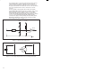
M/N 57C361 RESOLVER FROM MODULE Terminal Strip in Control Enclosure A REFERENCE ă2 B ă3 TO MODULE SINE D F G COSINE ă1 E REFERENCE VOLTAGE: 26 Vrms SINE VOLTAGE: 11.8 Vrms COSINE VOLTAGE: 11.8 Vrms ă4 ă5 ă6 ă7 ă8 ă9 10 Figure 3.3 Ć Typical M/N 57C361 Resolver Field Connections Step 6. Insert the cable assembly's (M/N 57C373) field terminal connector into the mating half on the module. Use a screwdriver to secure the connector to the module.
Monitor register 0. Verify that it contains numbers proportional to the shaft position of the resolver and that the numbers increase as the resolver is rotated clockwise. The direction of rotation can be reversed by switching the polarity of either the sine or the cosine wires. See figure 3.4.
3.3 Module Replacement WARNING INSERTING OR REMOVING THIS MODULE OR ITS CONNECTING CABLES MAY RESULT IN UNEXPECTED MACHINE MOTION. POWER TO THE MACHINE SHOULD BE TURNED OFF BEFORE INSERTING OR REMOVING THE MODULE OR ITS CONNECTING CABLES. FAILURE TO OBSERVE THESE PRECAUTIONS COULD RESULT IN BODILY INJURY. Use the following procedure to replace a module: Step 1. Turn off power to the rack and all connections. Step 2. Use a screwdriver to loosen the screws holding the connector to the module.
fafadfdfdasfdsfdsdsdfdsfdsfdsfsdfdsa afdfdsfdsfdfdsfdsfsadfda asfdfaddfdd
4.0 PROGRAMMING This section describes how the data is organized in the module and provides examples of how the module is accessed by the application software. For more detailed information refer to the DCS 5000 Enhanced BASIC Language Instruction Manual (JĆ3600). 4.1 Register Organization The input module contains a total of five 16Ćbit registers. Registers 0 and 1 contain resolver position data. The resolverĆtoĆdigital converter provides 12 bits of resolution.
bits 15 14 13 12 11 10 9 8 register 2 R R R R R R R R register 3 RW R R RW R R R R 7 6 R R RW RW 5 4 3 Ć Ć Ć Ć Ć Ć 2 R 1 R RW RW 0 R RW Interrupt line ID ăăă Interrupt allocated ăăăăInterrupt clock enable ăăăăInterrupt enabled Module fault ăResolver not connectedă ăăăăăCommon clock off Isolated power fault External strobe reset Position angle increasing External strobe status Interrupt flag status Figure 4.
Processor Module RESOLVER INPUT 57C411 275 W POWER SUPPLY POWER ON P S READY SYSTEM READY OK BLOWN FUSE NORMAL OK PROGRAM C B D E F G P3 D E F C B G LINK GND L2 L1 3 2 1 0 1 2 3 0 1 2 3 0 1 2 3 0 1 2 3 0 1 2 3 4 5 6 7 4 5 6 7 4 5 6 7 4 5 6 7 4 5 6 7 4 5 6 7 8 9 10 11 8 9 10 11 8 9 10 11 8 9 10 11 8 9 10 11 12 13 14 15 REMOTE 120V 0 1 2 3 6 7 8 FUSE BATTERY BACKĆUP 3 21 6 7 8 D E F C B G 12 13 14 15 D E F C B G 12 13 14 15 D E F C B G 12 13 14 15 D E F C B G 12 13 14
SYMBOLIC_NAME% Ć A symbolic name chosen by the user and ending with (%). This indicates an integer data type and all references will access register r". SYMBOLIC_NAME@ Ć A symbolic name chosen by the user and ending with (@). This indicates a boolean data type and all references will access bit number b" in register r". SLOT Ć Slot number that the module is plugged into. This number may range from 0Ć15. REGISTER Ć Specifies the register that is being referenced. This number may range from 0Ć4.
Remote I/O Slave Drop 7 Remote I/O Slave Drop 1 Remote I/O Slave Drop 2 I/O Module Master Rack Remote I/O Master Drop 0 Processor Module Figure 4.5 Ć Module in a Remote Rack 4.3.1 Single Register Reference Use this method to reference a 16Ćbit register as a single input. Resolver input data and update period registers are typically referenced using this method.
4.3.2 Bit Reference Use this method to reference individual inputs on the module. Common clock status and control bits are typically referenced using this method. The symbolic name of each bit should be as meaningful as possible: nnnnnăăRIODEF SYMBOLIC_NAME@[ MASTER_SLOT=m, ăăăăDROP=d, SLOT=s, REGISTER=r, BIT=b] where: nnnnn Ć BASIC statement number. This number may range from 1Ć32767. SYMBOLIC_NAME% Ć A symbolic name chosen by the user and ending with (%).
Each application program, or task, that wishes to reference the symbolic names assigned to the input module may do so by declaring those names COMMON. The frequency with which tasks read their inputs and write their outputs depends on the language being used. Control block tasks read inputs once at the beginning of each scan and write outputs once at the end of scan. BASIC tasks read an input and write an output for each reference throughout the scan.
2000 2010 4000 4001 4002 4998 4999 5000 5010 10000 UPDATE_TIME% = 1 \!500 microsecond conversion CCLK_EN@ = TRUE \!Turn on the clock ! ! Place any additional initialization software here ! ! Scan every 55 msec. ! CALL SCAN_LOOP( TICKS=10) CALL INVERTER( INPUT= RESOLVER_IN%,OUTPUT=READING%) END The symbolic names defined as COMMON" reference the inputs defined in the sample configuration task above. The symbolic name READING%" is local to the BASIC task and does not have I/O associated with it.
4.5.1 BASIC Task Example The following is an example of a BASIC task that handles interrupts from the input module defined in section 4.4. 1000 1005 1010 1020 1200 2000 2001 2002 2010 3000 3001 3002 3003 3004 3005 3006 3007 3008 3010 3011 4000 4001 4002 4003 4004 4005 4010 5000 5001 5002 6000 6001 6002 6003 6004 6005 6006 6007 6008 6009 6010 7000 7001 7002 7010 10000 4.5.
4000 4001 4002 4003 4004 4005 4010 5000 5001 5002 6000 6001 6002 6003 6004 6005 6006 6007 6008 6009 6010 7000 7001 7002 7010 10000 4.6 ! ! The following statement enables common clock from this module. ! If there is more than one interrupt task in a chassis, the task ! that enables common clock should always be the lowest priority ! task.
7025 7026 7027 7028 7029 7030 7036 7037 7039 7040 7046 7047 7048 7049 7050 7060 10000 4.7 ! ! The next statement calculates the distance ! traveled from the occurrence of the external ! event until this scan. ! CALL PULSE_MULT( INPUT=RESOLVER_IN%,ăăăă& RESET=-STROBE_RESET@,ăă& INITIAL_VALUE =RESOLVER_IN_EXT%, & MULTIPLIER=16385,ăăăăăăăăă& OUTPUT=EVENT_DISTANCE%) ! The next statement calculates the distance traveled ! from the last scan until this scan.
WARNING LOSS OF, OR OTHERWISE IMPROPER, RESOLVER SIGNAL CAN RESULT IN UNCONTROLLED MOTOR SPEED. PROVIDE AN INDEPENDENT METHOD OF SHUTTING DOWN EQUIPMENT IF THIS SHOULD OCCUR. FAILURE TO OBSERVE THIS PRECAUTION COULD RESULT IN BODILY INJURY AND IN DAMAGE TO, OR DESTRUCTION OF, THE EQUIPMENT. You must also determine the maximum safe operating speed for the motor, connected machinery, and material being processed.
5.0 DIAGNOSTICS AND TROUBLESHOOTING This section explains how to troubleshoot the module and field connections. 5.1 Incorrect Data Problem: The data is either always off, always on, or different than expected. The possible causes of this error are a module in the wrong slot, a programming error, or a malfunctioning module. It is also possible that the input is either not wired or wired to the wrong device. Use the following procedure to isolate the problem: Step 1.
If everything is working properly but the direction of rotation is backwards, it may be reversed by switching the polarity of either the sine or the cosine wires as shown in figure 3.4. Step 5. Verify that the input circuit is working properly. Connect an oscilloscope to the proper points on the terminal strip and confirm that the voltages are correct. The resolver reference voltage across TB 1 and 2 should be a nominal 26 Vrms. If it is 26 Vrms, check the jumpers on the terminal strip.
To test local I/O, first replace the input module. Next, replace the processor module (s). If the problem persists, take all of the modules except one processor module and the input module out of the backplane. If the problem is now corrected, one of the other modules in the rack is malfunctioning. Reconnect the other modules one at a time until the problem reappears. If none of these tests reveals the problem, replace the backplane.
programmer cannot monitor the inputs, the problem lies in the hardware (refer to step 4). Step 3. Verify that the user application program is correct. Registers 0 through 2 of the input module cannot be written to. If a BASIC task caused the bus error, the error log will contain the statement number in the task where the error occurred. If a control block task caused the error, you will need to search the task for any instances where you wrote to an input. Step 4.
5.3.1 No Interrupts Problem: The program does not execute, but no error codes are displayed on the processor module faceplate. If interrupts are never received by the application program and the timeout parameter in the event definition was disabled, the task will never execute. The watchdog timer for this module should never be disabled. Before you can determine why the program did not execute, you must first set the timeout parameter in the event definition.
5.3.4 Illegal Interrupt Detected Problem: All tasks in the chassis are stopped and error code 1F" appears on the faceplate of the processor module. A hardware interrupt has occurred but no event has been defined. Step 1. Verify that the user application program is correct. Verify that your interrupt response task contains an EVENT" statement that will be executed. Check carefully to determine whether a higher priority task is preventing the interrupt response task from running.
Appendix A Technical Specifications Ambient Conditions D Storage temperature: -40_ C Ć 85_ C D Operating temperature: 0_ C Ć 60_ C D Humidity: 5Ć90% nonĆcondensing Maximum Module Power Dissipation D 10 Watts Dimensions D Height: 11.75 inches D Width: 1.25 inches D Depth: 7.375 inches System Power Requirements D 5 Volts: 1700 ma D +12 Volts: 95 ma D -12 Volts: 95 ma Resolver Specifications D Frequency of operation: 2381 Hz D Minimum rotor impedance: 400 Ohms D Transformer ratio: 26/11.
fafadfdfdasfdsfdsdsdfdsfdsfdsfsdfdsa afdfdsfdsfdfdsfdsfsadfda asfdfaddfdd
Appendix B Module Block Diagram ADDRESS ID BUS ADDRESS BUS RESOLVER INPUT MODULE (57C411) ADDRESS DECODER TB I S O L A T I O N CONTROL LINES REFERENCE SINEWAVE GENERATOR 2381 Hz (+) REF OUT (+) GATE DATA BUS BUS 4mHz OSC CCLK CCLK TIMER COUNTER STROBE REF IN ĂI S O L A T TIMER INTERĆ RUPT LATCH 2 (-) CONTROL LOGIC GATE 1 3 4 (-) RESOLVER ANALOG TO DIGITAL CONVERTER ĂI O N (+) 5 6 SINE (-) (+) 7 COSINE 8 (-) EXTERĆ NAL TRIGĆ GER LATCH DIRECTION IPS OK ISOLATED +/- 15 VDC POWE
fafadfdfdasfdsfdsdsdfdsfdsfdsfsdfdsa afdfdsfdsfdfdsfdsfsadfda asfdfaddfdd
Appendix C Field Connections Pin No.
fafadfdfdasfdsfdsdsdfdsfdsfdsfsdfdsa afdfdsfdsfdfdsfdsfsadfda asfdfaddfdd
Appendix D Related Components 800123ĆR 800123ĆS 800123ĆT Ć Resolver (X1) (57C360) Ć Resolver (X2) Ć Resolver (X5) Designed for both footĆmounting and CĆface mounting. 800123Ć2R Ć Resolver (X1) (57C361) 800123Ć2S Ć Resolver (X2) 800123Ć2T Ć Resolver (X5) Designed for directĆcoupling. 57C373 Ć Terminal Strip/Cable Assembly This assembly consists of a terminal strip, cable, and mating connector. It is used to connect field signals to the faceplate of the input module.
fafadfdfdasfdsfdsdsdfdsfdsfdsfsdfdsa afdfdsfdsfdfdsfdsfsadfda asfdfaddfdd
fafadfdfdasfdsfdsdsdfdsfdsfdsfsdfdsa afdfdsfdsfdfdsfdsfsadfda asfdfaddfdd
Publication J-3640-1 - June 1990 Copyright © 2002 Rockwell Automation, Inc.. All rights reserved. Printed in U.S.A.