
Owner's manual


Rockwell Automation Publication 23P-UM001D-EN-P - July 2012 39
Stand Alone Regulator Installation, Wiring and Configuration Chapter 2
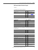
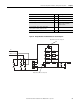
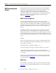
Figure 13 - Burden Resistor Jumpers (J4 and J5), Binary Gain Amp DIP Switches
(SW3 and SW4), and External Burden Resistor Terminal Block (XCT) Locations
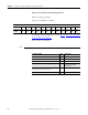
Figure 14 - Binary Gain Amp DIP Switch to Bit Layout
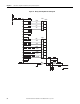
SW3 SW4
J5 J4
0VI RCT
XCT
MSB
LSB
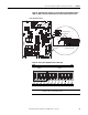
ON
Off
On
Pulse Transformer Board
Burden Resistor
Jumpers
External Burden Resistor
Terminal Block (XCT)
Binary Gain Amp
DIP Switches
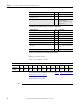
MSB LSB
Bit 11 Bit 10 Bit 9 Bit 8 Bit 7Bit 6Bit 5Bit 4Bit 3 Bit 2Bit 1Bit 0
IMPORTANT
The labels on DIP switches SW3 and SW4 do NOT correspond to the bit
numbers used to set the amplifier gain.
ON
1 2 3 4 1 2 3 4 5 6 7 8
SW3 SW4