
Instruction Manual

Publication 1794-6.5.8 - January 2010
70 Writing Configuration to and Reading Status from Your Module with a Remote I/O Adapter
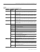
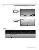
Word 5 PU FP CF 0 Reserved 0 0 0 0 0 BD DN 0
Word 6 0 0 0 0 P1 P0 0 0 0 0 V1 V0 W1 W0 U1 U0
Where:
PU = Power up unconfigured state
FP = Field power off
CF = In configuration mode
BD = Calibration bad
DN = Calibration accepted
P0 and P1 = Output holding in response to Q0 thru Q1
W0 and W1 = Wire off current loop status for input channels 0 and 1 respectively. (Not used on voltage outputs.)
U0 and U1 = Underrange for input channels o and 1 respectively.
V0 and V1 = Overrange for input channels o and 1 respectively.
Table 4.14
Analog Combo Module (1794-IF2XOF2I) Read
Table 4.15
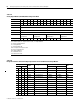
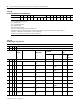
Configuring Your Input Channels
Input Channel Configuration
03 02 01 00 Set these bits for Channel 0
07 06 05 04 Set these bits for Channel 1
Bit Settings Input
Values
Data Format % Underrange
%Overrange
Input Range
(2)
Module Update
Rate
Hexadecimal Decimal (RTSI =
0)
(RTSI =
0)
IT = 1
0 0 0 0 Channel not configured
0 0 0 1 4–20mA signed 2’s complement 4% Under; 4%
Over
<0000–7878> <0000–30840> 7.5ms 5.0ms
0 0 1 0 ±10V signed 2’s complement 2% Under, 2%
Over
<831F–7CE1> <–31969–
31969>
2.5ms 2.5ms
0 0 1 1 ±5V signed 2’s complement 4% Under, 4%
Over
<8618–79E8> <–31208–
31208>
2.5ms 2.5ms
0 1 0 0 0–20mA signed 2’s complement
%
0% Under, 4%
Over
0–2710> 0–10000> 7.5ms 5.0ms
0 1 0 1 4-20mA signed 2’s complement
%
4% Under, 4%
Over
<0–2710> <0–10000> 7.5ms 5.0ms
0 1 1 0 0–10V signed 2’s complement
%
0% Under, 2%
Over
0–2710> 0–10000> 5.0ms 5.0ms
0 1 1 1 ±10V signed 2’s complement
%
2% Under, 2%
Over
<–D8F0–2710> <–10000–
10000>
5.0ms 5.0ms
1 0 0 0 0–20mA binary 0% Under, 4%
Over
0000–F3CF> 0000–62415> 2.5ms 2.5ms
1 0 0 1 4–
20mA
(1)
binary 4% Under, 4%
Over
0000–F0F1> 0000–61681> 7.5ms 5.0ms