# " !
Important User Information Because of the variety of uses for the products described in this publication, those responsible for the application and use of this equipment must satisfy themselves that all necessary steps have been taken to assure that each application and use meets all performance and safety requirements, including any applicable laws, regulations, codes and standards.
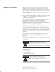
Identifies information that is critical for IMPORTANT successful application and understanding of the product. ATTENTION ! Environment and Enclosure This equipment is intended for use in a Pollution Degree 2 industrial environment, in overvoltage Category II applications (as defined in IEC publication 60664–1), at altitudes up to 2000 meters without derating. This equipment is considered Group 1, Class A industrial equipment according to IEC/CISPR Publication 11.
–3
Preface Purpose Use this manual to install and configure your FLEX I/OTM PROFIBUS Adapter, cat. no. 1794-APB Series B.
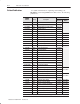
P–2 About this User Manual Related Publications For additional information on planning and installing your PROFIBUS system using FLEX I/O modules, refer to the following publications: Catalog Number Publications Voltage Description # (&*/+&$- $5$ Installation Instructions User Manual 9 9 " '& 0/530- (5 '$15(3 9 9 " '& ('6/'$/5 ('+$ 0/530- (5 '$15(3 9 9 " '& 0/530- (5 '$15(3 9 9 " '& ('6/'$
About this User Manual Publications Catalog Number Voltage 5 #" #" *,0/ +#0($ 5 5 #" #" 0/,0/ +#0($ 5 5 " *,0/ +#0($ 5 5 " 0/,0/ +#0($ 5 5 " .+( /$# *,0/ +#0($ 5 5 " .
P–4 About this User Manual
Table of Contents Overview of FLEX I/O and Your PROFIBUS Adapter Module Chapter 1 How Communication Takes Place and I/O Image Table Mapping Chapter 2 #,%6 6,-5 ,%36)4 216%-15 ,) $ :56)0 2716 %1( )028) :274 :56)0 %5-/: 36-21%/ '')5524-)5 2716-1+ -6 ;
Table of Contents (/138 $2 1) 9 1,05 ,*,5$. 0265 65265 1'6.( /$*( $%.( 9 " 9 921,05 ,4&3(5( 0265 1'6.( /$*( $%.( $22,0* 9 (/138 $2 9 921,05 ,4&3(5( 65265 1'6.( /$*( $%.( $22,0* 9 (/138 $2 9 ! 921,05 ,4&3(5( (.$8 65265 1'6.
Table of Contents 630%7)( 2%03+ 31&3 3(80) ; # )5-)6 1%+) %&0) %44-2+ 630%7)( 2%03+ 31&3 3(80) ; # )%( 32*-+85-2+ $385 2487 ,%22)06 )77-2+ 7,) 2487 -07)56 "35( -7 )6'5-47-326 *35 7,) ; # 2%03+ 31&3 3(80)
toc-iv Table of Contents Troubleshooting Chapter 5 $ - -$%, $ *-!+ )(- %(, +). &!,$))-%(# 0%-$ -$! ( % -)+, %!0%(# - -., "+)' -$! ,-!+ , )("%#.+ -%)( )"-0 +! Specifications Appendix A *! %"% -%)(, Device Data Base File Hazardous Locations )/!' !+ Appendix C 1 + ).
Overview of FLEX I/O and Your PROFIBUS Adapter Module What this Chapter Contains The FLEX I/O System This chapter describes: • what the FLEX I/O system is and what it contains • how to mount and remove your system easily • optional accessories • mounting dimensions and spacing requirements • the 1794-APB FLEX I/O PROFIBUS Adapter • adapter components • how to connect power wiring FLEX I/O is a small, modular I/O system for distributed applications that performs all of the functions of rack-ba
1–2 Overview of FLEX I/O and Your PROFIBUS Adapter Module Mount and Remove your System Easily You can horizontally or vertically mount the FLEX I/O system on a standard DIN rail. The adapter and terminal base easily snap on the DIN rail by hand. Refer to the installation instructions shipped with these components. Screw holes are also provided to horizontally or vertically panel-mount your system in an enclosure. To panel-mount your FLEX I/O system, use the optional mounting kit (1794-NM1).
Overview of FLEX I/O and Your PROFIBUS Adapter Module 1–3 ATTENTION Do not use more than one cable per system. ! Mounting Kit (1794ĆNM1) Use the optional 1794-NM1 mounting kit to mount your system on a panel or wall without a DIN rail.
1–4 Overview of FLEX I/O and Your PROFIBUS Adapter Module Mounting Dimensions and Spacing Requirements Inches (Millimeters) 1794ĆAPB 6 6 6 6 A /2).-!+ .3-2)-' )2 1794ĆTB2, ĆTB3 6 6 6 6 !)+ C //0.6),!2%+7 &.0 #!"+% .0 &.0 #!"+% &0., 3//%0 #.--%#2.0 %!130% (%0% &.
Overview of FLEX I/O and Your PROFIBUS Adapter Module Purpose of the 1794ĆAPB FLEX I/O Adapter 1–5 The 1794-APB is a FLEX I/O adapter that interacts with the FLEX I/O backplane and any PROFIBUS DP master/scanner controller on a PROFIBUS DP network. The 1794-APB module is a slave device to the DP master/scanner, and is a master controller of the FLEX I/O system where it is installed.
1–6 Overview of FLEX I/O and Your PROFIBUS Adapter Module PROFIBUS Adapter Components The adapter module consists of the following components: • • • • two diagnostic indicators PROFIBUS DP network connector 24V dc power wiring connection terminals two node address switches )#3 0. ,++#!/, '+"'! /, %-##+ -#" '+"'! /, %-##+ -#" "! 2'-'+% ,++#!/',+ #-*'+ ). #/2,-( ,++#!/,- ,"# ""-#.. 2'/!&#.
Overview of FLEX I/O and Your PROFIBUS Adapter Module 1–7 Network Connector Use the 9-pin D-shell connector to connect your adapter to the PROFIBUS network. Setting the Node Address Switches Set the node address using the 2-position thumbwheel switch. Valid settings range from 01 to 99. Use a pen to press either the + or – buttons to change the number. 24V DC Adapter 1794-APB/B !.1*,& *))! .*, 2+%) 2-$!'' 1%,%)# *))! .%*) !,(%) ' * ! ,!- 1%.
1–8 Overview of FLEX I/O and Your PROFIBUS Adapter Module
Chapter 2 How Communication Takes Place and I/O Image Table Mapping What this Chapter Contains Communication Over the I/O Backplane In this chapter, you will learn about: • communication over the FLEX I/O backplane (between the PROFIBUS adapter and the I/O modules) • how data is mapped into the I/O image table One 1794-APB PROFIBUS adapter can interface with up to eight terminal base units with installed FLEX I/O modules, forming a FLEX I/O system of up to eight slots.
2–2 How Communication Takes Place and I/O Image Table Mapping For example, a 16 point discrete input module will have up to 2 read words and 1 write word. I/O Image Input Size $& $& ' ,%$ #( ' & ( #%)( $ )! Output Size $& $& Module Image Inputs Not used Not used ! + " ! + " Check the I/O map for each module for the exact mapping. Polled I/O Structure The first word of output data received by the adapter is the Adapter Status Word.
How Communication Takes Place and I/O Image Table Mapping 2–3 Adapter Input Status Word The input status word consists of: • I/O module fault bits – 1 status bit for each slot • node address changed – 1 bit (+/ (+/ (+/ (+/ (+/ (+/ (+/ (+/ +#0($ 0(/ '/. '/ $.$-1$# +#$ ##-$.. & *%$# '/ The adapter input status word bit descriptions are shown in the following table. Bit Description Bit Explanation &'. !'/ '. .
2–4 How Communication Takes Place and I/O Image Table Mapping Possible causes for an I/O module fault are: • • • • • transmission errors on the FLEX I/O backplane a failed module a module removed from its terminal base incorrect module inserted in a slot position the slot is empty The node address changed bit is set when the node address switch setting has been changed since power up. The new node address does not take effect until the adapter has been powered down and then powered back up.
How Communication Takes Place and I/O Image Table Mapping 2–5 1794ĆIB8 - 8Ćpoint Digital Input Module Image Table Mapping I/O Image Module Image Input Size Read Not used )+ )+!, Inputs Not used Output Size Write %&-"+ %'" Not used )+ )+! 1794ĆIB8 Memory Map Decimal Bit 15 14 13 12 11 10 09 08 07 06 05 04 03 02 01 00 Size Octal Bit 17 16 15 14 13 12 11 10 07 06 05 04 03 02 01 00 Read Words " ! )+! )- .
2–6 How Communication Takes Place and I/O Image Table Mapping 1794ĆIB16 - 16Ćpoint Digital Input Module Image Table Mapping I/O Image Module Image Input Size Read Inputs *, *,"- Not used Output Size Write &'.#, &(# Not used *, *," &'.
How Communication Takes Place and I/O Image Table Mapping 2–7 1794ĆOB8 - 8Ćpoint Discrete Output Module Image Table Mapping I/O Image Input Size Read Module Image %' %' Not used Output Size Not used Outputs %' %' ( Write Not used 1794ĆOB8 Memory Map Decimal Bit 15 14 13 12 11 10 09 08 07 06 05 04 03 02 01 00 Octal.
2–8 How Communication Takes Place and I/O Image Table Mapping 16Ćpoint Source Input Module Image Table Mapping - 1794ĆIV16 I/O Image Input Size Read Module Image ') ') Inputs Output Size Write $ / #% Not used Not used ') ') * Not used Memory Map of 16-Point Input Module Image Table – 1794-IV16 Dec. Bits Oct.
How Communication Takes Place and I/O Image Table Mapping 2–9 16Ćpoint Digital Sink Output Module Image Table Mapping 1794ĆOV16 I/O Image Input Size Read Module Image !# !# Not used Output Size Outputs !# !# $ Write Not used Memory Map of 16-Point Digital Sink Output Module Image Table – 1794-OV16 Dec. Bits 15 14 13 12 11 10 09 08 07 06 05 04 03 02 01 00 Size Oct.
2–10 How Communication Takes Place and I/O Image Table Mapping 1794ĆIB8S - 8Ćpoint Discrete Sensor Input Module Image Table Mapping I/O Image Module Image Input Size Read Status ,. ,.#/ Inputs Not used Output Size Write $) 4 (*$ Not used ,. ,.
How Communication Takes Place and I/O Image Table Mapping 2–11 1794ĆOB8EP - 8Ćpoint Discrete Protected Output Module Image Table Mapping I/O Image Input Size Read Module Image .0 !.0% Overload Fault Bits Output Size Not used Outputs .0 !.0%1 Write Not used Not used Dec. Bits 15 14 13 12 11 10 09 08 07 06 05 04 03 02 01 00 Size Oct. Bits 17 16 15 14 13 12 11 10 07 06 05 04 03 02 01 00 Read/Write Words &1&04&% 1&& -.
2–12 How Communication Takes Place and I/O Image Table Mapping 1794ĆIA8 - 8Ćpoint Discrete Input Module Image Table Mapping Module Image I/O Image Input Size Read Not used )+ )+!, Inputs Not used Output Size Write %&-"+ %'" Not used )+ )+! 1794ĆIA8 Memory Map Decimal Bit 15 14 13 Octal Bit 17 16 15 12 11 10 09 08 14 13 12 11 10 Not used 07 06 05 04 03 02 01 00 07 06 05 04 03 02 01 00 Read Words " ! )+! Not used " ! )
How Communication Takes Place and I/O Image Table Mapping 2–13 1794ĆOA8 - 8Ćpoint Discrete Output Module Image Table Mapping I/O Image Module Image Input Size ') ') Read Not used Output Size Write Not used ') ') * Outputs Not used 1794ĆOA8 Memory Map Decimal Bit 15 14 13 12 11 10 09 08 07 06 05 04 03 02 01 00 Oct.
2–14 How Communication Takes Place and I/O Image Table Mapping 1794ĆIE8 Series B - 8 Input Analog Module Module Image Input Data Channel 0 Input Data Channel 1 I/O Image Input Data Channel 2 Input Size Input Data Channel 3 Input Data Channel 4 0, ,.#/ Input Data Channel 5 Input Data Channel 6 Input Data Channel 7 Underrange PU Configure select Not used Output Size Not used ,. ,.
How Communication Takes Place and I/O Image Table Mapping 2–15 1794ĆIE8/B Range Selection Bits Channel No. Decimal Bits (Octal Bits) Channel 0 Channel 1 Channel 2 Channel 3 Channel 4 Channel 5 Channel 6 Channel 7 F0 C0 F1 C1 F2 C2 F3 C3 F4 C4 F5 C5 F6 C6 F7 C7 00 08 (10) 01 09 (11) 02 10 (12) 03 11 (13) 04 12 (14) 05 13 (15) 06 14 (16) 07 15 (17) ! &% . .
2–16 How Communication Takes Place and I/O Image Table Mapping Word (* Decimal Bit Definition #,+ Underrange bits (U) (* #' #.# - % " '' %+ (4Ć20mA current input only) #, (** +)(' + ,( #')-, " '' % #, (** +)(' + ,( #')-, " '' % ' +( (' " ' + , #' # , + #," * *($ ' (* () ' #')-, /#* (* #')-, -** ', %(/ 2 & #,+ 2 (, -+ + , ,( #, Power Up bit - included in series B modules only. This bit is 0 in series A modules.
How Communication Takes Place and I/O Image Table Mapping 2–17 1794ĆOE4 Series B - 4 Output Analog Module Image Table Mapping I/O Image Input Size Module Image -/ -/# Read PU Diagnostics Not used Analog Data Channel 0 Analog Data Channel 1 Analog Data Channel 2 Analog Data Channel 3 Not used Output Size Write MC Full Range Config.
2–18 How Communication Takes Place and I/O Image Table Mapping 1794ĆOE4/B Range Selection Bits (Write Word 6) Channel No. Decimal Bit Channel 0 Channel 1 Channel 2 Channel 3 F0 C0 F1 C1 F2 C2 F3 C3 00 08 01 09 02 10 03 11 / ! &% / ; 51 ! &% (( 10(+)63' 4'.'%5 $+5 6.. 3#0)' $+5 "*'0 %10(+)63'& 51 1(( +0&+7+&6#. %*#00'.4 8+..
How Communication Takes Place and I/O Image Table Mapping Word ') ') * +!), ') ') ') ') 2–19 Decimal Bit (Octal Bit) Definition "+* Full range bits (F) ') "& "-" , $ ! && $* "+ ')) *('& * +' ',+(,+ ! && $ "+ ')) *('& * +' ',+(,+ ! && $ & *' '& "+* 0 '+ ,* * + +' "+* 0 Configure select bits (C) ') "& "-" , $ ! && $* "+ ')) *('& * +' ',+(,+ ! && $ "+ ')) *('& * +' ',+(,+ ! && $ & *' '& "+* 0 0 '+
2–20 How Communication Takes Place and I/O Image Table Mapping 1794ĆIE4XOE2 Series B - Analog Combo Module Image Table Mapping Module Image I/O Image Input Data Channel 0 Input Size Input Data Channel 1 40 "02&3 Read Input Data Channel 2 Input Data Channel 3 Underrange & Diag.
How Communication Takes Place and I/O Image Table Mapping 2–21 1794ĆIE4XOE2 Range Selection Bits Channel No.
2–22 How Communication Takes Place and I/O Image Table Mapping Word Write Word 1 ,." Decimal Bit (Octal Bit) '0/ '0/ '0/ '0/ Channel 0 analog data sign bit. Channel 1 analog data 6 '0 )#$0 (1/0'$'#" 03, / !,*-)#*#+0 +1* #. 1+1/#" ),3#. '0/ .# 5#., 6 * 1/#/ )) '0/ Channel 1 analog data sign bit. '0/ '0/ ,0 1/#" /#0 0, '0/ Full range bits (F) $,. '+"'2'"1 ) !& ++#)/ '0 !,..#/-,+"/ 0, '+-10 !& ++#) '0 !,..
How Communication Takes Place and I/O Image Table Mapping 2–23 1794ĆIR8 - RTD Input Analog Module Image Table Mapping Module Image Reserved Input Data Channel 0 Input Data Channel 1 I/O Image Input Data Channel 2 Input Size Input Data Channel 3 Input Data Channel 4 1- -/#0 Input Data Channel 5 Input Data Channel 6 Input Data Channel 7 Overrange Underrange Calibration Status Configuration Calibration Mask Output Size RTD Type 1- -/#0 RTD Type 1794ĆIR8 Read Dec.
2–24 How Communication Takes Place and I/O Image Table Mapping 1794ĆIR8 Word/Bit Descriptions Word Dec. Bits (Octal Bits) Description (* + *.
How Communication Takes Place and I/O Image Table Mapping Word Write word 1 Dec. Bits (Octal Bits) 2–25 Description Module Data Type Bit 01 00 + !"# 0(/ + &,+( - +0*/. . ("! "/2""* *! *&,+( - +0*/. . ("! "/2""* *! Enhanced mode select - )" .0-". 1+(/ $" !-+, -+.. ,-" &.&+* -".&.
2–26 Word -&/# +-" How Communication Takes Place and I/O Image Table Mapping Dec. Bits (Octal Bits) Description % **#( 3,# Bit 03 02 01 00 RTD Type - Range #.&./ *!# "#$ 0(/ + .#*.+- !+**#!/#" "+ *+/ .! * +%) / α /+ + #.
How Communication Takes Place and I/O Image Table Mapping 2–27 1794ĆIT8 - Thermocouple Input Module Image Table Mapping Module Image Reserved Input Data Channel 0 Input Data Channel 1 I/O Image Input Data Channel 2 Input Size Input Data Channel 3 0, ,."/ Input Data Channel 4 Input Data Channel 5 Input Data Channel 6 Input Data Channel 7 Overrange Underrange Calibration Status Output Size Configuration Calibration Mask 0, ,.
2–28 How Communication Takes Place and I/O Image Table Mapping 1794ĆIT8 Word/Bit Descriptions Decimal Bit (Octal Bit) Word Description ! *, !-!,0! ! *, $ ))!' )+/. . ! *, $ ))!' )+/. . ! *, $ ))!' )+/. . ! *, $ ))!' )+/. . ! *, $ ))!' )+/. . ! *, $ ))!' )+/. . ! *, $ ))!' )+/. .
How Communication Takes Place and I/O Image Table Mapping Word 0)2% .0$ Decimal Bit (Octal Bit) Description Module Data Type Bit 01 00 Definition . $%&!3+2 . )/.+!0 #.3-21 1#!+%$ "%25%%- !-$ -)/.+!0 #.3-21 1#!+%$ "%25%%- !-$ )2 Fixed Digital Filter - (%- 2()1 ")2 )1 1%2 ! 1.&25!0% $)')2!+ &)+2%0 )1 %-!"+%$ ()1 &)+2%0 1%22+%1 2. .
2–30 Word /(1% -/$ How Communication Takes Place and I/O Image Table Mapping Decimal Bit (Octal Bit) Description '!,,%* '%/+-#-2.*% 5.
How Communication Takes Place and I/O Image Table Mapping 2–31 Thermocouple/RTD Input Module (1794ĆIRT8) Image Table Mapping Module Image Input Data Channel 0 Input Data Channel 1 I/O Image Input Data Channel 2 Input Size 40 Input Data Channel 3 #02'3 Input Data Channel 4 Input Data Channel 5 Input Data Channel 6 Input Data Channel 7 Overrange Underrange Channel Faults RFlg CJC Diagnostics EDT command and response Output Size Data Format 40 #02'3 FM Reference Jct Filter Cut TC/RTD Mode Se
2–32 How Communication Takes Place and I/O Image Table Mapping 15 14 13 12 11 10 09 08 07 06 05 04 03 02 01 00 Size 17 16 15 14 13 12 11 10 07 06 05 04 03 02 01 00 Read/Write Words ''3&4 ) ''3&4 ) ''3&4 ) ''3&4 ) ''3&4 ) $0.."/% ''3&4 ) ''3&4 ) ''3&4 ) $0.."/% %"4" !2*4& !2*4& Bit/Word Definitions for the Block Transfer Words for the TC/RTD/mV Input Module Word Dec.
How Communication Takes Place and I/O Image Table Mapping Word Dec. Bits (Octal Bits) "3,5( "13' 2–33 Description Input Filter Cutoff bits ,5 ,.5(3 ,/( 1045$054 $&56$. ),.5(3,0* '(2(0'4 10 5+( /1'6.( 4 /1'( 1) 12(3$5,10 $3'8$3( ),.5(3,0* 10.: '()$6.5 ),.5(3,0* /4 /4 /4 /4 4 4 4 ,54 Reference Junction 64(' 8+(0 ,0265 5:2( ,4 4(5 51 5+(3/1&162.( $0' 4(0413 /1'( ,4 4(5 51 ,05(30$. &1/2(04$5,10 (54 $ ),9(' 3()(3(0&( -60&5,10 51 &1/2(04$5( $.. 5+(3/1&162.( &+$00(.
2–34 How Communication Takes Place and I/O Image Table Mapping Word "3,5( "13' Dec. Bits (Octal Bits) ,54 Description Sensor Type (Thermocouple or RTD) RTD Type ,5 (0413 582( )13 &+$00(.4 5+316*+ (4,45$0&( '()$6.5 1+/ 5 α 631 51 1 1+/ 5 α 631 51 1 1+/ 5 α 51 1 1+/ 5 α 51 1 1+/ ,&-(.
How Communication Takes Place and I/O Image Table Mapping Word Dec. Bits (Octal Bits) $-, 2–35 Description Sensor Mode Select bits $- !(,)+ ') ! ,!&! - ")+ # ((!&, Thermocouple 1-!+( & )'*!(, -$)( .,!, )& %.( -$)( ,!(,)+, (-!+( & )'*!(, -$)( .,!, -#! / &.! ,!&! -! ")+ 3+!"!+!( ! %.( -$)( ,!&! -$)( ) )'*!(, -$)( - $, +!"!+!( ! -) ) $""!+!(-$ & '! ,.+!'!(- !-0!!( # ((!&, RTD 40$+! () )'*!(, -$)( 40$+! 0$-# .
2–36 How Communication Takes Place and I/O Image Table Mapping Word $6.8* $46) (438 (438 Dec. Bits (Octal Bits) .87 Description Sensor Type (Thermocouple or RTD) RTD Type .8 *3746 8=5* +46 (-&33*17 8-649,- *7.78&3(* )*+&918 4-2 8 α 964 84 4 4-2 8 α 964 84 4 4-2 8 α " 84 4 4-2 8 α " 84 4 4-2 .
How Communication Takes Place and I/O Image Table Mapping Word ,&." *,! *). *). ,&." *,! ,&." *,! Dec. Bits (Octal Bits) &.- 2–37 Description Input Type Select &. )+/. .3+" -"'" .&*) #*, % ))"'- %",(* */+'" *. /-"! RTD loop resistance offset select bits - /-"! 1%") &)+/. .3+" &- -". .* )! -")-*, (*!" -"'" . &- -". .* 41&," 1&.% '**+ ,"-&-. ) " *(+")- .&*) ''*1- 3*/ .* -". .%" .
2–38 How Communication Takes Place and I/O Image Table Mapping 4 Input Isolated Analog Module (Cat. No.
How Communication Takes Place and I/O Image Table Mapping Dec.
2–40 How Communication Takes Place and I/O Image Table Mapping Configuring Your Input Channel Input Channel Configuration 03 02 01 00 Set these bits for Channel 0 07 06 05 04 Set these bits for Channel 1 11 10 09 08 Set these bits for Channel 2 15 14 13 12 Set these bits for Channel 3 Input Values Bit Settings % Underrange/ % Overrange Data Format Input Range2 Hexadecimal Decimal Module Update Rate (RTSI = 0) (RTSI = 0), IT=1 0 0 0 0 Channel not configured 0 0 0 1 4-20mA
How Communication Takes Place and I/O Image Table Mapping Word $ # -/# $ # -/# /(1$ -/# /(1$ -/# Decimal Bit (Octal Bit) 2–41 Definition (10 $0$/3$# (10 Calibration Done bit (DN). '(0 !(1 (0 0$1 1- %1$/ " *(!/ 1(-, "5"*$ (0 "-+.*$1$# (1 Calibration Bad bit (BD). '(0 !(1 (0 0$1 1- (% 1'$ "' ,,$* " *(!/ 1(-, "-$%%("($,10 " ,,-1 !$ 0 3$# -/ !$ /$ # ./-.
2–42 How Communication Takes Place and I/O Image Table Mapping Word Decimal Bit (Octal Bit) 1)3% .1$ Channel Configuration (refer to Configuring Your Input Channel ) 1)3% .1$ 1)3% .1$ 4"+)#!3).- ; .5%,"%1 Definition )32 Channel 0 Configuration )32 Channel 1 Configuration )32 Channel 2 Configuration )32 Channel 3 Configuration )32 Real Time Sample Interval - 1.'1!,2 3(% )-3%15!+ .
How Communication Takes Place and I/O Image Table Mapping Decimal Bit (Octal Bit) Word 0(2$ -0# 0(2$ -0#1 ,# 2–43 Definition (2 Transparent bit (TR). '(1 !(2 5'$, 1$2 2- .$0+(21 "-,%(&30 2(-, 2- !$ "' ,&$# 5(2'-32 31(,& 2'$ !(2 (2 $2 2- (2 Initiate Configuration bit (IC). '$, 1$2 (,1203"21 2'$ +-#3*$ 2- $,2$0 "-,%(&30 2(-, +-#$ 0$1$,2 "-,%(&30 2(-, # 2 .0(-0 2- -0 "-(,"(#$,2 5(2' !$(,& 1$2 ,"$ 0$230,1 2- 2'$ "-,%(&30 2(-, (1 ..
2–44 How Communication Takes Place and I/O Image Table Mapping Word/Dec.
How Communication Takes Place and I/O Image Table Mapping 2–45 Word/Bit Descriptions for the 1794-OF4I Isolated Analog Output Module Read Words Decimal Bit (Octal Bit) ,." '0/ Read Back Channel 0 1.'+% +,.* ) ,-#. 0',+ '0 '/ !,-4 ,$ 0&# ,10-10 ,$ !& ++#) 1.'+% + 0. +/'0',+ '0 '/ 0&# !,+"'0',+ ,$ 0&# ,10-10 / "#0#.*'+#" 4 +" # " !( '/ + '* %# ,$ 3& 0 0&# 1/#. & / /#+0 / ,10-10 0, 0&# *,"1)# +, !&#!(/ .# -#.$,.*#" ,+ 0&# " 0 ,.
2–46 How Communication Takes Place and I/O Image Table Mapping Write Words Decimal Bit (Octal Bit) Definition *21 .2 31&% *2 Safe State Source bits (S1/S0). !)&- *1 2)&1& #*21 %&1*(-"2& 2)& 1.30$& .' 2)& 1"'& 12"2& %"2" *2 #*2 0&1&2 .32/321 2. , 31&% 5*2) 7 *2 #*2 ).+% .32/32 "2 *21 $300&-2 +&4&+ 31&% 5*2) 7 *2 #*2 "'& 12"2& %"2" *1 *- .32/32 %"2" 5.0%1 *2 Output enable bit (EN). !)&- 1&2 2)& .
How Communication Takes Place and I/O Image Table Mapping Write Words Word 7 Decimal Bit (Octal Bit) Bit 00-03 Words 8 and 9 Definition Channel calibration selection bit. When this bit is set (1), the channel can be calibrated using the calibration clock bit (CK). Bit 00 corresponds to output channel 0, bit 01 corresponds to output channel 1, it 02 corresponds to output channel 3, bit 03 corresponds to output channel 4 Bit 04 Gain/Offset selection bit (GO).
2–48 How Communication Takes Place and I/O Image Table Mapping Isolated Analog Combo Module (1794ĆIF2XOF2I Series B) Image Table Mapping Module Image I/O Image Input Data Channel 0 Input Size Input Data Channel 1 0, ,."/ Read Read Back Output Data Channel 0 Read Back Output Data Channel 1 Real Time Sample PU FP CF BD DN P1 P0 EN S1 S0 Output Size Write V1 V0 W1 W0 U1 U0 Set to 0 Output Data Channel 0 0, ,.
How Communication Takes Place and I/O Image Table Mapping 2–49 Word/Dec. Bit 15 14 13 12 11 10 09 08 07 06 05 04 03 02 01 00 Word/Octal Bit 17 16 15 14 13 12 11 10 07 06 05 04 03 02 01 00 Word 8 Where: Not Used PU = Power up unconfigured state FP = Field power off CF = In configuration mode BD = Calibration bad DN = Calibration accepted. P0 and P1 = Output holding in response to Q0 thru Q1 W0 and W1 = Wire off current loop status for input channels 0 and 1 respectively.
2–50 How Communication Takes Place and I/O Image Table Mapping Setting the Input Filters Bits $ ! Channel 03 02 01 00 Input Channel 0 07 06 05 04 Input Channel 1 A/D Conversion Rate Low Pass Filter # " # " # " # " # " # " # " #
How Communication Takes Place and I/O Image Table Mapping 2–51 Table 2.A Configuring Your Outputs for the 1794ĆIF2XOF2I Analog Combo Module Configuration Bits MSD LSD Nominal Range Data Type Output Values Hexadecimal Update Rate Decimal ; / '1/2.)/)05 # '1/2.)/)05 /4 # '1/2.)/)05 /4 ; / '1/2.)/)05 ; / '1/2.)/)05 ; # '1/2.)/)05 # '1/2.
2–52 How Communication Takes Place and I/O Image Table Mapping Decimal Bit (Octal Bit) Word .0$ )21 %1%04%$ )21 Calibration Done bit (DN). ()1 ")2 )1 1%2 2. !&2%0 ! #!+)"0!2).- #6#+% )1 #.,/+%2%$ )2 Calibration Bad bit (BD). ()1 ")2 )1 1%2 2. )& 2(% #(!--%+ #!+)"0!2).-- #.%&&)#)%-21 #!--.2 "% 1!4%$ .0 "% 0%!$ /0./%0+6 )21 %2 2. )21 %1%04%$ )2 %2 2. )2 Configuration mode bit (CF) ()1 ")2 )1 1%2 5(%- 2(% #!+)"0!2).- ,.
How Communication Takes Place and I/O Image Table Mapping Word Decimal Bit (Octal Bit) ,/" Input Channels 0 and 1 Filter Selections #$#/ 1, Setting the Input Filters ,/" ,/" ,/" ,/" Definition '10 Channel 0 Filter Setting '10 Channel 1 Filter Setting '1 2–53 #1 1, Channel Configuration '10 Input Channel 0 Configuration #$#/ 1, Configuring Your Input Channels '10 Input Channel 1 Configuration #$#/ 1, Configuring Your Input Channe
2–54 How Communication Takes Place and I/O Image Table Mapping Word Decimal Bit (Octal Bit) "03& %0/5+/6'& +54 "03& 6$-+%#5+0/ =! 07'.$'3 Definition Request for hold outputs (Q). *#//'- 3'26'45 $+54 5*#5 +/4536%5 #/ 065165 50 *0-& +54 065165 -'7'- 8*'/ 53#/4+5+0/4 (30.
How Communication Takes Place and I/O Image Table Mapping 2–55 Incremental Encoder Module (1794ĆID2) Image Table Mapping Module Image I/O Image R PD1 PD0 S1 S0 C1 C0 G1 Z1 B1 A1 G0 Z0 Input Size Store 0 - Saved Counter Value on channel 0 ,( (* + Store 1 - Saved Counter Value on channel 1 B0 A0 Channel 0 - current counter value on channel 0 Channel 1 - current counter value on channel 1 Channel 0 - Counter word readback Channel 1 - Counter word readback Code for identification of sof
2–56 How Communication Takes Place and I/O Image Table Mapping Word Bit " ! +.! +*0 ! &0 Definition Status for input G ,1(/" 0. */)&00". %&/ &0 3%"* /"0 &*!& 0"/ /&$* ( 0 &0 Cal 0 %&/ &0 3%"* /"0 &*!& 0"/ 0% 0 +1*0". % / ""* (& . 0"! %&/ &0 &/ ."/"0 4 ( "/"0 &0 Cal 1 %&/ &0 3%"* /"0 &*!& 0"/ 0% 0 +1*0". % / ""* (& . 0"! %&/ &0 &/ ."/"0 4 ( "/"0 &0 Store 0 %&/ &0 3%"* /"0 &*!& 0"/ +1*0".
How Communication Takes Place and I/O Image Table Mapping Word &81:&68, Bit 1:9 2–57 Definition 65:863 65:863 =68, .68 9-::15/ :0- .;5+:165 6. +6;5:-8 6,- #-3-+:165 *1:9 6;5:15/ 65 7691:1<- 81915/ -,/- 6. 157;: 91/5)3 %7 ,=5 +6;5:15/ ,-:-8415-, *? !;),8):;8- -5+6,-8 ' !;),8):;8- -5+6,-8 ' !;),8):;8- -5+6,-8 ' 6;5:15/ ;7 65 :0- 7691:1<- -,/- 6. 157;: 91/5)3 )5, ,6=5 65 7691:1<- -,/- 6. 157;: 91/5)3 6 +6;5: .
2–58 How Communication Takes Place and I/O Image Table Mapping Word $6/8+ $46* Bit Definition Channel 1 Control Word 438641 ;46* ,46 7+88/3- 8.+ ,93)8/43 4, )4938+6 /87 /8 Mode Selection bits 4938/3- 43 547/8/:+ 6/7/3- +*-+ 4, /3598 7/-3'1 "5 *;3 )4938/3- *+8+62/3+* (= 9'*6'896+ +3)4*+6 % 9'*6'896+ +3)4*+6 % 9'*6'896+ +3)4*+6 % 4938/3- 95 43 8.
How Communication Takes Place and I/O Image Table Mapping Word )+ +$ )+ , Bit 2–59 Definition Filter Selection $- Filter A0 enable - # ( -#$, $- $, , - ( ).(- + $, $( ') *.&, ).(-$(" ,$"( & $, !$&- + 1 $"$- & &)0 * ,, !$&- + 0$-# , & - & !$&- + )(,- (- $- Filter A1 enable - # ( -#$, $- $, , - ( ).(- + $, $( ') *.&, ).(-$(" ,$"( & $, !$&- + 1 $"$- & &)0 * ,, !$&- + 0$-# , & - & !$&- + )(,- (- $- 3 (.
2–60 How Communication Takes Place and I/O Image Table Mapping Pulse Counter Module (1794ĆIP4) Image Table Mapping Module Image I/O Image Counter 00 - 16-bit period measurement or low word of 32Ćbit period measurement for channel 0 Input Size Counter 01 - pulse counter for channel 0 or high word of 32Ćbit period measurement ($ $& ' Counter 10 - 16-bit period measurement or low word of 32Ćbit period measurement for channel 1 Counter 11 - pulse counter for channel 1 or high word of 32Ćbit period
How Communication Takes Place and I/O Image Table Mapping 2–61 (Octal Bit⇒) 17 16 15 14 13 12 11 10 07 06 05 04 03 02 01 00 Dec. Bit ⇒ 15 14 13 12 11 10 09 08 07 06 05 04 03 02 01 00 Word⇓ Write )(.,)& ), - & .- .# ' -/, !/( .$)( )(.,)& ), - .- .# &) % !, +/ ( 2 ( * ,$) '/&.$*& )(.,)& ), - .- .# -. ,. )! ( 1 ' -/, ' (. - ,0 # , *)-$.$0 " ' -/, ' (. , 2 !), .# , -* .$0 # (( & - . )( !), , -* .
2–62 Word +$ )+ How Communication Takes Place and I/O Image Table Mapping Bit Control Word 0 - )(-+)& 0)+ !)+ , --$(" -# !.( -$)( )! ).(- + $-, Pulse counting and period time measurement selection for Channel 0 *.&, ).(-$(" ( * +$) -$' ' ,.+ ' (- , & - * +$) -$' ' ,.+ ' (- , & - $-, Pulse counting and period time measurement selection for Channel 1 *.&, ).(-$(" ( * +$) -$' ' ,.+ ' (- , & - * +$) -$' ' ,.
How Communication Takes Place and I/O Image Table Mapping Word Bit % ' #% ' Start new measurement bit - Channel 0 * " & ' &' %' " * ! &(% ! "' #" $#& ' ) ' Start new measurement bit - Channel 1 * " & ' &' %' " * ! &(% ! "' #" $#& ' ) ' Start new measurement bit - Channel 2 * " & ' &' %' " * ! &(% ! "' #" $#& ' ) ' Start new measurement bit - Channel 3 * " & ' &' %' " * ! &(% ! "' #" $#& ' ) ' Reset Counter, Channel 0 - $#&
2–64 How Communication Takes Place and I/O Image Table Mapping 1203ĆFM1 - SCANport Module Image Table Mapping I/O Image Module Image 0//'%4+0/ 4#453 *#//'- Read 0//'%4+0/ 4#453 *#//'- 0)+% 4#453 *#//'- "02&3 /#-0) ''&$#%, *#//'- 0)+% 4#453 *#//' /#-0) ''&$#%, *#//' "02& 0//'%4+0/ /#$-' *#//'- 0//'%4+0/ /#$-' *#//'- Write 0)+% 0..#/& *#//'- "02&3 /#-0) '('2'/%' *#//'- 0)+% 0..
How Communication Takes Place and I/O Image Table Mapping 2–65 Connection Enable Word Definition Connection Enable Channel 2 *3 /3 2&% Connection Enable Channel 1 /3 2&% Description 0/13 $)"..&, &."#,& #*3 )&. 2&3 3/ 3)& -/%4,& 6*,, "33&-03 3/ $/..&$3 3/ 3)& 0/13 %&5*$& )&. 1&2&3 3/ 3)& -/%4,& 23/02 $/--4.*$"3*.( 6*3) 3)& $/..&$3&% 0/13 %&5*$& )*2 424",,7 $"42&2 3)& %&5*$& 3/ '"4,3 0/13 $)"..&, &."#,& #*3 )&.
2–66 How Communication Takes Place and I/O Image Table Mapping Module Defaults for: Adapter Defaults Optimal Sizes Catalog Number Description Input Default Output Default Input Default Output Default & ("-%# +(% ,#" ')-, ("-%# +(% ,#" -,)-, ("-%# +(% ,#" (& ( ("-%# '!*#&#', % '!("#* ("-%# -%+# (-',#* ("-%# / )(*, ("-%# The default val
Chapter 3 Connect the Adapter to the PROFIBUS DP Network What this Chapter Contains The DP Physical Layer This chapter describes: • the DP physical layer • using line types A and B • equipment you need • how to connect the adapter to the network • how to terminate the network The PROFIBUS network media is a balanced transmission line corresponding to the standard EIA RS-485, terminated at both ends. Both line A and line B types are available, depending on your system requirements.
3–2 Connect the Adapter to the PROFIBUS DP Network Cabling and Equipment Required for Line A Type Line A cabling can support baudrates as high as 1.5M bits/s. Cables You need a shielded twisted pair cable for your cabling (bus segments or drop cables). Any line A cable available on the market can be used to connect your adapter to a PROFIBUS network. TĆjunction Connectors You need t-junction connectors to connect your droplines to bus segments. You can use any t-junctions available on the market.
Connect the Adapter to the PROFIBUS DP Network Cabling and Equipment Required for Line B Type 3–3 Line B cabling can support baudrates as high as 500k bits/s. Cables You need a shielded twisted pair cable for your cabling (bus segments or drop cables). Any shielded twisted pair cables available on the market can be used to connect your adapter to a PROFIBUS network, however, bus segment cables must contain wire for data ground and a cable braid shield.
3–4 Connect the Adapter to the PROFIBUS DP Network Connect the Adapter to the Network For line A or B connections, use bus segments with t-junctions and termination blocks to form the PROFIBUS media (trunk cable). Use termination blocks to terminate the line at each end of the trunk cable. Use drop cables to connect devices to the network. The maximum number of stations on the same network is 32. 0./ !+$ 31 $&,$-2 $01.- + .,/32$0 5(2' .-%(&30 2(. .%25 0$ 12$0 " --$0 .-20.
Connect the Adapter to the PROFIBUS DP Network 3–5 3. Insert the wired connector into the mating connector on the PROFIBUS adapter. Terminate the Network You must use termination blocks only if your devices on the end of the network do not have built-in terminating resistors. Terminate the PROFIBUS media (trunk cable) at both ends of the network. If you are not using a connector with built-in resistors, terminate the cable at the adapter connector as shown below.
3–6 Connect the Adapter to the PROFIBUS DP Network
Chapter 4 Configure the Adapter for Master/Slave Communication What this Chapter Contains In this chapter, we describe: For Information on: See Page !( $% # $ ' ! & % ! % $ " % # &$ # " # % # % % # ! &# % ! % ! &# % ! # $"! $ % How Master/Slave Communication Takes Place !( A data exchange between the master and slave cannot be performed until check configuration and send parameter data are issued.
4–2 Configure the Adapter for Master/Slave Communication Entering User Parameter Data Send parameter data is comprised of a string of octets (1–32) that contain 244 bytes of data: • octets 1–7 contain data specific to the: – PROFIBUS standard – defaults contained in the database (GSD) file • octets 8–32 are user configurable and contain user parameter data.
Configure the Adapter for Master/Slave Communication 4–3 If the send parameter data is received with no user parameter data, the flags byte is set to zero which selects: • auto configure • reset outputs to zero on fault • reset inputs to zero on fault The reserved bits must be set to zero to prevent undesired firmware update behavior. This is the default behavior of the module as defined in the GSD file.
4–4 Configure the Adapter for Master/Slave Communication Condensed Format The condensed format consists of the flags byte and the module key parameter for each of the eight slots. This parameter dictates which I/O module must be installed.
Configure the Adapter for Master/Slave Communication 4–5 The following table shows the identification numbers for current FLEX I/O modules. FLEX I/O Module Catalog Number Module Identification Number (module key) *.+20*+# *#.'$, 2 % 2 % 2 % 2 % 2 % 2 % 2 % 2 % 2 % 2 % 2 % &1-$$)20*+# *#.
4–6 Configure the Adapter for Master/Slave Communication When you use the condensed format, no safe state data can be defined, thus the safe state data is left at the power up default of all zeroes. Setting the Fault Action in the byte to Use Safe State with this format is the equivalent of setting Reset to Zero.
Configure the Adapter for Master/Slave Communication 4–7 Data format for Full Format Name Size Description Module Key WORD Module ID that must be installed1 Module Data BYTE Bits 0-3 Safe State Size (in words) Sizes2 Bits 4-7 Config Size (in words) Safe State Data ARRAY Output Safe States. Word array of size Safe State Size. Module ARRAY FLEX Module Configuration. Word array of size Config Configuration Data Size. 1 Only bits 0-12 are used.
4–8 Configure the Adapter for Master/Slave Communication Entering Check Configuration Data On a PROFIBUS DP network, the I/O data exchanged between the PROFIBUS DP master and a DP slave is encapsulated into logical modules. The total I/O data exchanged between a PROFIBUS DP master and a DP slave device comprises a set of logical modules which is defined in the check configuration data. Each physical slot of the FLEX I/O system is represented by two logical modules (one input and one output).
Configure the Adapter for Master/Slave Communication 4–9 The identifier byte and its format are described in the following illustration. This byte is defined in Part 3 of the PROFIBUS standard. -12 )',)&)#!,2 )2 )2 3+"%0 %!12 )',)&)#!,2 )2 #-,#)12%,#6 -4%0 "62% -0 5-0$ 5(-*% *%,'2( *%,'2( "62% 5-0$ &-0+!2 "62% 1203#230% 5-0$ 1203#230% %,'2( -& $!2! "62% 0%1. • • • "62% 0%1. 5-0$ 5-0$1 ),.32 -32.32 1.%#)&)# )$%,2)&)%0 &-0+!21 ),.32 -32.32 ),.32 -32.
4–10 Configure the Adapter for Master/Slave Communication Check Configuration Example ! ! " Name , , , , , , , , , , , , , , , , , , , , Identifier Description Byte # , ,-+ (* $')-, /(* # -,)-, , ,-+ (* (-,)-, /(* # %(, $')-, &( -% /(* + # %(, (-,)-, &( -% /(* # %(, $')-, &( -% &),0 # %(, (-,)-, &( -% /(* # %(, $')-, &( -% /(* +
Chapter What this Chapter Contains Troubleshooting with the Indicators 5 In this chapter, we describe how to use the adapter’s indicators for troubleshooting. Locate the two bi-color indicators on the front panel of the adapter. They show both normal operation and fault conditions in your Flex I/O PROFIBUS system.
5–2 Troubleshooting Viewing Status from the Master's Configuration Software You can use read diagnostics to view status using the master’s configuration software. The adapter returns identification in response to the Read DP–Slave Diagnostic Information message. Read DP-Slave Diagnostics Information Message Octet Description !0% ! !' .! % #)*-.% $! !, 2.! $ !0%-%*) %)*, !0%-%*) &*, +.!, . ./ %. * ! ,!-- $ )#! %.
Specifications - FLEX I/O PROFIBUS Adapter Module, 1794ĆAPB Series B I/O Capacity 8 modules Input Voltage Rating 24V dc nominal Input Voltage Range 19.2V to 31.2V dc (includes 5% ac ripple) Communication Rate All rates up to 12.
A–2 Specifications Specifications - FLEX I/O PROFIBUS Adapter Module, 1794ĆAPB Series B PROFIBUS Connector 9Ćpin DĆshell PROFIBUS Drop Cable Standard drop cable Power Conductors Wire Size Category Agency Certification (when product is marked) 12 gauge (4mm2) maximum solid or stranded copper wire rated at 75oC or greater 3/64 inch (1.2mm) insulation max.
What this Chapter Contains This PROFIBUS adapter requires a (GSD) file for implementation. This file is available for downloading from www.ab.com/networks/gsd/. The GSD file is used by your configuration tool to help you set up your system. Your configuration tool automatically reads the GSD file and extracts defaults used in the data exchange.The file is in ASCII format and you can view it with any text editor.
B–2 Device Data Base File (GSD)
The following information applies when operating this equipment in hazardous locations: 41&7%65 /#4-'& = ! #4' 57+6#$.' (14 75' +0 .#55 +8+5+10 41725 #0& #<#4&175 1%#6+105 #0& 010*#<#4&175 .1%#6+105 10.; #%* 241&7%6 +5 5722.+'& 9+6* /#4-+0)5 10 6*' 4#6+0) 0#/'2.#6' +0&+%#6+0) 6*' *#<#4&175 .1%#6+10 6'/2'4#674' %1&' "*'0 %1/$+0+0) 241&7%65 9+6*+0 # 5;56'/ 6*' /156 #&8'45' 6'/2'4#674' %1&' .19'56 = 07/$'4 /#; $' 75'& 61 *'.
C–2 Hazardous Locations
This Glossary contains terms specific to Allen-Bradley and PROFIBUS FMS and DP. AllenĆBradley communication defaults values used for communication configuration data such as OD, CRL ( for FMS) DP slave database,and bus parameters whenever the coprocessor’s working RAM configuration is reinitialized. application layer the seventh layer of the seven-layer OSI reference model. This layer is where the coprocessor first interacts with the application program.
G–2 communication relationship in FMS, defines all the parameters for the communication between two nodes. configuration management in FMS, set of FMA 7 services to upload and download the PROFIBUS bus parameters, CRL, and to read SAP status and station identification. connector header a connector that attaches between the processor and coprocessor and provides communication between the two modules. connection type in FMS, the type of connection between two nodes.
G–3 defined connection in FMS, a connection type that specifies both end nodes of the channel by giving their network address and the FDL service access points (SAPs) used in both nodes diagnostics three LED indicators located on the front panel of the coprocessor provide the user with the status of the coprocessor and its communication channels. Also referred to as user interface. domain object in FMS, represents a portion of the processor’s memory image.
G–4 FMS interface a 9-pin female D-shell connector located at Port 1 on the front panel of the coprocessor. FMS Physical Access Addressing FMS option that allows the access of data at a physical address by specifying the address in the service. FMS Symbolic Access Addressing FMS option that allows to statically associate a symbolic name or short reference number (or index) with a physical address within a node.
G–5 LSAP or SAP Link layer Service Access Point. A logical sub-addresses within devices that allow the distribution of communication flow over dedicated tasks, depending on the required processing. FMS uses LSAPs indifferently to define generic communication relationships between two devices (logical communication channels). DP uses predefined LSAPs to access specific functions or services between masters and slaves. master initiates transfer of messages without any prior remote request.
G–6 open at the initiator in FMS, a connection type where the source service access point (SAP) is shared among several communication relationships (associated with a different destination address and SAP). The device uses only one of these relationships at a time, depending on the selected remote node. open at the responder in FMS, a connection type where the destination address and service access point (SAP) are undefined, thus making the connection available to any device.
G–7 power supply module that supplies power to the I/O chassis containing the processor and coprocessor and other modules processor Any one of the family of Allen-Bradley Programmable Logic Controllers that support the coprocessor interface: PLC-5/11 , -5/20 , -5/30 , -5/40 , -5/60 and -5/80 . processor interface a 58-pin connector located on the left side of the coprocessor that uses a PLC-5 Connector Header to attach to the processor for communication between the two modules.
G–8 station an address or software location on the network. Also referred to as node. SET command in a MSG instruction, allows transfer of an element, an array of elements or an FMS structure to or from a node on the network. slave are only allowed to transmit immediate acknowledge or immediate response to master requests. At the Link Layer level, any master can access any slave without restrictions. Also referred to as passive stations or adapters.
Index # /3$1 ""$22.1($2 ! "*/+ -$ ".,,4-(" 3(.- ".,/.-$-32 ".--$"3 3. 3'$ -$36.1* # 3 $7"' -&$ #(,$-2(.-2 -# 2/ "(-& 1$04(1$,$-32 2314"341$ (-23 ++(-& (-#(" 3.12 , ).1 ".,/.-$-32 ,.#4+$ .5$15($6 ,.4-3(-& -# 1$,.5(-& -$36.1* ".--$"3.1 -.#$ ##1$22 26(3"'$2 /41/.2$ 1$ # -# 61(3$ 6.1#2 2/$"(%(" 3(.-2 6(1(-& !(3 .1# #$2"1(/3(.-2 !(3 6.1# #$2"1(/3(.-2 !+."* 31 -2%$1 1$ # !+.
I–2 Index 9 9 ! 3#0 2$1 ,$25-0) "-,,$"2-0 ,$25-0) +$#( 1.$"(%(" 2(-,1 .'71(" * * 7$0 $62$,#$0 " !*$ %(*2$0 2(+$1 9 %* &1 !72$ # .2$0 .30.-1$ ! ").* ,$ "-++3,(" 2(-, "-+.-,$,21 # .2$0 +-#3*$ 2$0+(, * ! 1$ $62$,#$0 " !*$ +-#3*$ #$% 3*21 +-3,2(,& #(+$,1(-,1 +-3,2(,& )(2 -.2(-, * ""$11-0($1 . ,$* +-3,2(,& 1. "(,& 0$/3(0$+$,21 1712$+ "-,%(&30 2(-, $6 +.
Index ; ; ; ; ; ; ; ; ; ; ; ! '8#.1-' '81-#/#4+0/ +.#)' 4#$-' .#11+/) �# ; " ; ; .#34'2 3-#6' %0..5/+%#4+0/ .#8+.5. -+/' -'/)4* .'.029 .#1 ; " ; .'.029 .
I–4 Index ($ ' % ' , ($ ' ' ! & , (& % $ % ! ' % ' ('# #" (% #%! ' #" "& #%! ' & +' #%! '& ( #%! ' ) %' !#("' " ( ' #" , #) ! % * % " $' % * % " #"" ' #" ' %! " & * % " #"" ' #"& $' % '# %#$ *#% && "! "'& # '% "& % % *#% ' & % $' #"& "$(' &' '(& *% ' *#% &
I–2 55/7D ;+.5/B + #8-4@/55 >=86+=387 ><37/<< 2+< ,//7 2/59371 3=< -><=86/;< 369;8?/ 9;8.>-=3?3=B +7. :>+53=B 08; 68;/ =2+7 B/+;< (/ ./<317 6+7>0+-=>;/ +7. <>998;= + ,;8+. ;+71/ 80 +>=86+=387 9;8.>-=< @8;5.@3./ %2/B 37-5>./ 5813- 9;8-/<<8;< 98@/; +7. 68=387 -87=;85 ./?3-/< 89/;+=8; 37=/;0+-/< <=;+53+ • ><=;3+ • +2;+37 • /513>6 • ;+C35 • >51+;3+ • +7+.