
User Manual

Application ConsiderationsC–2
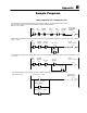
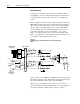
Circuit Overview
To make sure your signal source and the 1771-VHSC module are
compatibility, you need to understand the electrical characteristics of
your output driver and its interaction with the 1771-VHSC input
circuit.
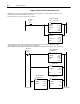
Refer to Figure C.1. The most basic circuit would consist of R1, R2,
JPR4, JPR5, the photodiode and associated circuitry around half of
the opto-isolator. The resistors provide first-order current limiting to
the photodiodes of the dual high speed opto-isolator. With JPR4
closed, and JPR5 open, the total limiting resistance is R1 + R2 =
1150 ohms. This jumper position is designated “12 to 24 Volt
Range.” Assuming a 2V drop across the photodiode and R97 and
R98, you would have 8.7-19mA demanded from the driving circuit
as the applied voltage ranged from 12 to 24V.
Figure C.1
Example Circuits for 5V Differential and +12 to +24V SingleEnded
Drivers
R1 R2
C41
JPR4 JPR5
JPR6
JPR7
JPR8 JPR9
JPR10
JPR11
R3 R4
R97 R98
C43
Q2
Q3
D2
D3
D5
D6
R100
R101
R31
R36
C38
C42
+5V
C3 C4
1
2
3
4
5V DIFFERENTIAL
LINE DRIVER
+12 TO 24V
INPUT
HIGH
LOW
DRIVE
DRIVE
1501K
R
1501K
22 ohm
Input Terminals
Voltage
Jumpers
V
oltage Jumpers
Filter Jumpers
10691I
Drive
Circuit
D1
D4
40.2
40.2
40.2
40.2
+12 TO 24V
SINGLEENDED
DRIVER
In the “5 Volt” position (JPR4 open; JPR5 closed), R1 is shorted and
the limiting resistance is 250 ohms. If 5.0V was applied at the input,
the current demanded would be (5.0 - 2.0)/150 = 20mA.
The above type of calculation is necessary to the user since the
driving device must cause a minimum of 5mA to flow through the
photodiode regardless of which jumper position is selected.