Allen Bradley Proportional/Inte gral/Derivative Control (2-Loop) Module (Cat. No.
Table of Contents Introduction . . . . . . . . . . . . . . . . . . . . . . . . . . . . . . . . . . . . 1 1 General . . . . . . . . . . . . . . . . . . . . . . . . . . . . . . . . . . . . . . . . . . . 1 1 Assembly and Installation . . . . . . . . . . . . . . . . . . . . . . . . . 2 1 General . . . . . . . . . . . . . . . . . . . . . . . . . . . . . . . . . . . . . . . . . . . Hardware Description . . . . . . . . . . . . . . . . . . . . . . . . . . . . . . . . . Internal Selections . . . . . . . . . .
ii Table of Contents Worksheets . . . . . . . . . . . . . . . . . . . . . . . . . . . . . . . . . . . . A 1 Application Example 1, Continuous Block Transfer . . . . . . B 1 General . . . . . . . . . . . . . . . . . . . . . . . . . . . . . . . . . . . . . . . . . . . Example Application . . . . . . . . . . . . . . . . . . . . . . . . . . . . . . . . . . B 1 B 1 Application Example 2, Periodic Block Transfer . . . . . . . . . C 1 General . . . . . . . . . . . . . . . . . . . . . . . . . . . . . . .
Chapter 1 Introduction General The Proportional/Integral/Derivation Control (2-loop) Module Assembly (cat.no.1771-PD) is an intelligent I/O module that performs closed loop PID control. The PID module is a process controller. The PID module monitors the analog input process variable, compares the input to the desired set point, and calculates the analog output control variable based on the control algorithm programmed in the module.
Chapter 1 Introduction Capabilities The PID module can control one or two PID closed loops. The two loops can be independent or linked together by and advanced control function such as cascade or decoupling. Expanded loop features can be chosen in addition to standard features to suite the application. All features are software selectable with the exception of the I/O range, the source of +5V DC, and the fault response to a hardware failure (which are selected using internal programming plugs).
Chapter 1 Introduction download an output bias from the PC processor Expanded control features perform scaling on the process variable, set point and/or error set minimum and maximum scaling values use the tieback as the feedforward input take the square root of the feedforward input add a feedforward offset multiply the feedforward term by a constant perform lead/lag filtering on the feedforward term download a feedforward value from the PC processor cascade the output of loop 1 into the set point of loop
Chapter 1 Introduction manual control station of both loops to manual control. The module’s analog inputs can be read and outputs can be set by the PC processor. The PID module can draw its +5V DC operating power from either the chassis backplane power supply or from a user-supplied +5V DC power supply through the field wiring arm. The external power supply option permits a more fault tolerant system by allowing the PID module to be powered independently.
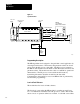
Chapter 1 Introduction Figure 1.
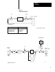
Chapter 1 Introduction Figure 1.2 System Overview 1771 – P1 Supply 1771 – PD Module PC Processor or Adapter Optional User Supplied Manual Control Station Manual Request Man/Auto Status Block Transfer Analog Output (V) X Tieback Input Analog Input (PV) 1770 – P1 supply P r o c e s s + – 15V DC 100mA +5V DC 1.2A Optional Supply 11092 Programming Description The PID algorithm can be adapted to the particular control application by selecting desired features.
Chapter 1 Introduction PC processor operation is changed from run mode to program or test mode a PC processor fault occurs a communications cable break occurs between the PC processor and the I/O chassis Each loop can be programmed independently to one of the following responses when a soft fault occurs: set the analog output to minimum value (+4mA or +1V DC) holds the analog output to the last value before the soft fault occurre performs PID control based on the last values transferred to the module befor
Chapter 1 Introduction The last level of fault tolerance results from powering the module from external +5V DC and + l5V DC power supplies, independent of I/O chassis backplane power, through the field wiring arm. Application in Control Systems The PID module performs closed loop control. Once programmed, it can operate independently of the PC processor. System status and alarm information can be reported to the PC processor to ensure safe system performance. Redundant control is another alternative.
Chapter 1 Introduction Figure 1.3 Levels of Distributed Control Data Highway 1771 - PD P r o c e s s 1771 - PD 1771 - PD P r o c e s s P r o c e s s Manual Control Station 1771 - PD P r o c e s s 1771 - PD P r o c e s s 1771 - PD P r o c e s s P r o c e s s 11100 The PID module can also be used in a system with adaptive control based on the PC processor’s ability to constantly adjust the control algorithm in the module.
Chapter 1 Introduction Finally, PID modules can be used in distributed control schemes. The data highway can be used to link PC processors which are controlling PID modules. Figure 1.3 shows the various levels of distributed control. Manual Overview The remainder of the manual explains different aspects of PID module operation.
Chapter 2 Assembly and Installation General The PID module must be configured internally and wired externally to suite the conditions under which the module will be used. Module and power supply specifications are listed at the end of this chapter. Hardware Description The PID module is a dual-slot module. The left front panel contains three LED indicators, the right front panel contains a write-on label that can be used to record the voltage or current range and the most recent date of calibration.
Chapter 2 Assembly and Installation Table 2.A Indicator Diagnostics Indicator State FAULT (red) OFF Normal operation. ON Hardware fault. Analog outputs are held at either last state, minimum or maximum value as determined by the user selected programming plugs.
Chapter 2 Aseembly and Installation Calibration of the I/O ranges should be checked yearly to maintain specified accuracy. Programming Plugs and Locations The PID module contains two printed circuit boards. The left-hand board is the digital board, the right-hand board is the analog board. Programming plugs are located on both the analog and digital circuit boards inside the PID module. Typically they stand higher than the surrounding components on the circuit board.
Chapter 2 Assembly and Installation Selection Procedure (Part A) Begin with digital board features using Table 2.B. 1. The hard fault response of the module is selected first. A hard fault occurs when a module failure is detected in the event of a failure, the analog output will either maintain the last value or will be set to the minimum or maximum value. A single choice is made for both outputs as to whether they hold last value or go to minimum/maximum.
Chapter 2 Aseembly and Installation Table 2.C Programming Plug Selections: Analog (right hand) Board Choose and record the required conditions for each function below.
Chapter 2 Assembly and Installation Table 2.D Programming Plug Positions: Analog (right hand) Board Mark the programming plug position for each function below.
Chapter 2 Aseembly and Installation Location Function Position E23 [3] +5V dc from backplane +5V dc from external source TOP BOTTOM E24 [3] +5V dc from backplane +5V dc from external source TOP BOTTOM *or loss of +5V dc [1] IN refers to connecting the two pins together. OUT refers to storing the programming plug by placing it over a single pin, electrically floating. [2]The positions of programming plugs E18, E21 and E22 must be the same.
Chapter 2 Assembly and Installation 5. Choose the tieback input 1 as voltage or current. If tieback input 1 is wired to track the manual control station associated with analog output 1, then both tieback input 1 and analog output 1 must be selected to the same mode of either current or voltage. 6. Choose analog input 2 as voltage or current. 7. Choose analog output 2 as voltage or current. 8. Choose tieback input 2 as voltage or current.
Chapter 2 Aseembly and Installation Part C) Record the required programming plug positions on table 2.D using your selections on table 2.C for reference. Select LEFT/RIGHT, IN/OUT or TOP/BOTTOM so that Table 2.D has a position defined for every E location. 1. Using your selections inTable 2.C for reference, mark the corresponding plug positions in the right-hand column of Table 2.D Table 2.D.
Chapter 2 Assembly and Installation 2. Refer to Figure 2.3 to identify the locations of the user-selectable and factory configured programming plugs. 3. Starting at E1, read down table 2.D and set each programming plug on the analog board. CAUTION: The programming plugs at location E11 and E12 could interfere with the front cover flange when the analog board is re-assembled to the rest of the module. This could happen when either the E11 or E12 programming plug is placed in the OUT (floating) position.
Chapter 2 Aseembly and Installation Figure 2.2 Programming Plug Locations (Digital Board) Backplane Connector Backplane Connector E 5* No Plug E6 * E1 * E4 Jumper Test Pins StakePin Connector E7 * Hold Max Min Hold Last State E10 E8 * E3 * E9 * Diagnostic Indicators * Programming Plug Pin Factory Configured Plug 11101 Figure 2.
Chapter 2 Assembly and Installation External Connections Terminal identification of the PID module’s field wiring arm and general connections are shown in Figure 2.4. Typical I/O connections for a single closed loop configured in current mode are shown in Figure 2.5. The remaining three figures show typical connections to input and output devices and control mode connections to a manual control station. Figure 2.6 shows typical connections to input devices without a manual control station.
Chapter 2 Aseembly and Installation Figure 2.4 Terminal Identification and Connections Terminal Identification Cat. No. 1771-PDC Terminal 18 17 16 15 14 13 12 11 10 9 8 7 6 5 4 3 2 1 1 2 3 4 5 Function Input 1 (+ Lead) Input 1 (- Lead) Input 2 (+ Lead) Input 2 (- Lead) Tieback Input 1 Tieback Input 2 Analog Output 1 Module Common Analog Output 2 +15V DC + - 15V DC Common -15V DC Manual Mode 1 Manual Mode 2 Manual Request OPT.
Chapter 2 Assembly and Installation Figure 2.5 Typical Connections for 1 Loop Control PID Module Power Supply - + General Manual Control Station TERMINAL IDENTIFICATION CAT. NO. 1771-PDC TERMINAL FUNCTION 18 INPUT 1 (+LEAD) 17 INPUT 1 (-LEAD) 16 INPUT 2 (+LEAD) 15 14 INPUT 2 (-LEAD) 13 TIEBACK INPUT 2 12 ANALOG OUTPUT 1 11 MODULE COMMON 10 9 ANALOG OUTPUT 2 7 6 MANUAL MODE 1 5 4 MANUAL MODE 2 3 OPT.
Chapter 2 Aseembly and Installation Figure 2.6 Connections to Input Devices PID Module TERMINAL IDENTIFICATION CAT. NO. 1771-PDC TERMINAL FUNCTION 18 INPUT 1 (+LEAD) 17 INPUT 1 (-LEAD) 16 15 INPUT 2 (+LEAD) INPUT 2 (-LEAD) 14 TIEBACK INPUT 1 13 TIEBACK INPUT 2 12 ANALOG OUTPUT 1 11 MODULE COMMON 10 8 ANALOG OUTPUT 2 + 15V DC +- 15V DC COMMON 7 - 15V DC 6 MANUAL MODE 1 5 4 MANUAL MODE 2 9 3 MANUAL REQUEST OPT.
Chapter 2 Assembly and Installation Figure 2.7 Connections to Output Actuators PID Module TERMINAL IDENTIFICATION CAT. NO. 1771-PDC TERMINAL FUNCTION 18 INPUT 1 (+LEAD) 17 INPUT 1 (-LEAD) 16 15 INPUT 2 (+LEAD) INPUT 2 (-LEAD) 14 TIEBACK INPUT 1 13 TIEBACK INPUT 2 12 ANALOG OUTPUT 1 11 MODULE COMMON 10 8 ANALOG OUTPUT 2 + 15V DC +- 15V DC COMMON 7 - 15V DC 6 MANUAL MODE 1 5 4 MANUAL MODE 2 9 3 MANUAL REQUEST OPT.
Chapter 2 Aseembly and Installation Figure 2.8 Control Mode Connections to Manual Control Station PID Module TERMINAL IDENTIFICATION CAT. NO. 1771-PDC TERMINAL FUNCTION 18 INPUT 1 (+LEAD) 17 INPUT 1 (-LEAD) 16 15 INPUT 2 (+LEAD) INPUT 2 (-LEAD) 14 TIEBACK INPUT 1 13 TIEBACK INPUT 2 12 ANALOG OUTPUT 1 11 MODULE COMMON 10 8 ANALOG OUTPUT 2 + 15V DC +- 15V DC COMMON 7 - 15V DC 6 MANUAL MODE 1 5 4 MANUAL MODE 2 9 3 MANUAL REQUEST OPT.
Chapter 2 Assembly and Installation allows the PID output to be switched open at the manual control station and a manually controlled output to be switched into the system. When in manual mode, care should be taken not to return to automatic control when the output is below +1V dc or +4mA. If attempted, an output surge could occur. The PID module performs a bumpless transfer when the tieback input is tracking a signal at or above the minimum level of +1V dc or +4mA.
Chapter 2 Aseembly and Installation Figure 2.
Chapter 2 Assembly and Installation +15V dc Analog Supply When both the module outputs and tieback inputs (if used) are configured in current mode, additional compliance can be selected. As such, module common is internally connected to -15V dc. The +15V dc analog power supply can provide a 30 V dc source to the input current loop by jumpering the +15V Dc terminal of the PID module to the positive lead of the current transmitter (Figure 2.10).
Chapter 2 Aseembly and Installation Figure 2.10 Current Mode Input Using External +15V dc Supply Two-Wire Transmitter +4 to +20mA PID Module 1771-PD (+) (-) TERMINAL IDENTIFICATION CAT. NO. 1771-PDC TERMINAL FUNCTION 18 INPUT 1 (+LEAD) 17 INPUT 1 (-LEAD) 16 INPUT 2 (+LEAD) 15 14 INPUT 2 (-LEAD) 13 TIEBACK INPUT 2 12 ANALOG OUTPUT 1 11 MODULE COMMON 10 9 ANALOG OUTPUT 2 7 6 MANUAL MODE 1 5 4 MANUAL MODE 2 3 OPT.
Chapter 2 Assembly and Installation or indicating instrument if used (typically 250 ohms) must be considered when calculating the voltage drop in the loop. For example, the required voltage for an input loop that contained the PID module, manual control station, and current transmitter that requires at least 18V dc would be 18V +2 (250 ohms) (.020 amps)= 18V +10V = 28V dc.
Chapter 2 Aseembly and Installation welders which generate high electrical noise. Equipment grounding can carry electrical noise when ground loops exists. The alternate grounding method is for instruments, only. A instrument ground bus is located inside the enclosure containing the I/O chassis, manual control station, and PC processor. The instrument bus is electrically isolated from the I/O chassis and enclosure.
Chapter 2 Assembly and Installation Internal Fusing The PID module has internal pico fuses to protect circuitry from surges in the optional +5V dc supply., A blown fuse condition is indicated when none of the front panel LED indicators turn on after you turn on this supply. If the LEDs do not turn on, check programming plugs E23 and E24. These plugs allow you to select the source of +5V dc from the backplane or from an external supply.
Chapter 2 Aseembly and Installation Place PID modules in one or more chassis containing only PID modules. Supply +5V dc to each PIC module using one or more optional external power supplies. Place an on/off switch in the +5V dc lead to each PID module. This allows you to remove power and replace a PID module without turning off power to other PID modules in the chassis.
Chapter 2 Assembly and Installation Plastic keying bands shipped with the I/O chassis should be used. The position of the keying bands on the upper backplane connector must correspond to the mating slots on the module connector. Refer to Figure 2.11.
Chapter 2 Aseembly and Installation Figure 2.11 Keying Diagram Single Module Group 0 PID Module 1 Upper Backplane Connectors Keying Bands 2 4 6 8 10 12 14 16 18 20 22 24 26 28 30 32 34 36 Left Connector Power Supply Specifications 2 4 6 8 10 12 14 16 18 20 22 24 26 28 30 32 34 36 Right Connector 11106 Isolation must be maintained between the analog and digital circuits of the PID module to minimize electrical noise interference.
Chapter 2 Assembly and Installation Table 2.E Customer + 15V dc Power Supply Requirements Specifications +15 Volts 15 Volts Output Current 100mA 100mA Output Voltage Tolerance 1% 1% Regulation (type) Series Series Line Regulation (for 10V AC input change) +0.2% +0.2% Load Regulation (no load to full load) +1.0% +1.
Chapter 2 Aseembly and Installation Module Specifications The PID module specifications are listed in Table 2.G. Table 2.G Specifications Process Variable Inputs Digital Resolution Number 12 binary, 1 part in 4095 process variable input 1 Accuracy Configuration Input Impedance Differential 250 ohms (current) Range (user selectable) +4 to +20mA 4.
Chapter 2 Assembly and Installation 125V dc (voltage) Temperature Coeffeicient 10mA maximum load current.
Chapter 3 Programming General Before starting to program the PID module, read this entire chapter thoroughly. Be sure that the programming plug functions have been selected as described in section titled Programming Plug Selection. The PID module can be programmed in four general steps: 1. Choose the PID module features required for the application. These are listed in section titled Capabilities (chapter 1) and are presented in the algorithm flow chart (Figure 3.15). 2.
Chapter 3 Programming Section titled Programming Consideration explains the application of block transfer instructions. Section titled Expanded Features describes the expanded features of the PID module and how they can be applied. Additionally, four appendices contain helpful programming information: Appendix A contains the worksheets which are used to record data that is entered into the PC processor and transferred to the PID module.
Chapter 3 Programming features. The full algorithm flow chart is presented in section titled Algorithm Flow Chart. The PID module (rev C or later) uses the ISA algorithm (P, I and D dependent gains) or the Allen-Bradley algorithm (P, I and D independent gains). Refer to appendix E for algorithm comparison and selection. Earlier revision modules use only the Allen-Bradley algorithm. Figure 3.
Chapter 3 Programming The status block SB is a read block transfer file used to report the current status of the PID module and any alarm condition detected by the module. The transfer of the status block is also used to prompt the next write block transfer. Figure 3.2 illustrates the multiple block concept. Figure 3.
Chapter 3 Programming Figure 3.
Chapter 3 Programming The PID module prompts the sequencing of block transfers. The write block transfer instruction in the user program contains the data table address of the first word of the block file to be transferred. By manipulating this address, different data block files can be transferred with the same write block transfer instruction. There are three control bits which are associated with the handshaking of the load/enter sequence.
Chapter 3 Programming Figure 3.4 Load/Enter Sequence Status Command Load Bit Enter Bit Block Transfers read write Ready Bit 0 1 0 0 1 0 0 1 0 1 0 1 P R O C E S S O R 1st SB 1st The processor reads the status block to start the sequence. 2nd DB 2nd The processor writes the dynamic block to the PID module (load bit set) to transfer dynamic block data. 3rd SB 3rd The processor reads the status block to confirm dynamic block data and to address the next block transfer.
Chapter 3 Programming Word and Bit Definitions This section defines the words and bits of the three write blocks and the single read block. For ease of reference, the following word and bit notation is used throughout the manual: A PID module word is abbreviated as Wxx. Example: Word number 12 = W12. A PID module bit is abbreviated as Bxx. Example: Bit number 07 = B07. The word and bit abbreviations can be used together. Example: Word number 12, Bit number 07 = W12 B07.
Chapter 3 Programming dynamic block, loop blocks and status block are listed in Table 3.J, Figure 3.13 and Figure 3.14 found at the end of section title Word and Bit Definitions. Table 3.
Chapter 3 Programming such as feedforward, scaling, lead/lag, and all the words in the loop block must have a value. The value of unused expanded feature words must be zero. W01 B13 Calibration. Reset to 0 selects normal operation. Set to 1 only for calibrating the module. This bit is examined only at power-up, and is used with W02 B17 and B16.
Chapter 3 Programming Figure 3.
Chapter 3 Programming W01 B12 Binary/BCD Format. [LE] Reset to 0 selects the 4-digit BCD (4095 maximum) format. Set to 1 selects the 12-bit are listed in Table 3.B. Table 3.
Chapter 3 Programming by (LE). These bits are protected from accidental change because they control the number of PID loops, standard or expanded loop features and binary or BCD data format. These bits can be changed in the same manner that loop constants are changed, only by a load/enter sequence. The remaining bits in the master control word and the remaining dynamic block words can be changed at any time by a write block transfer.
Chapter 3 Programming W02 B00 PID Algorithm. Reset to 0 the PID module uses A-B gain values. Set to 1 the PID module uses ISA values. W03 Dynamic Block Start Address. This word contains the data table address of the first word in the file associated with the dynamic block. The address is required by the PID module to prompt the transfer of the dynamic block. W04 Loop 1 Block Start Address. This word contains the data table address of the first word in the file associated with the loop 1 block.
Chapter 3 Programming W08 Bias 1, BIAS1. When using only standard loop features, the loop bias is the value stored in this word. When expanded loop features are selected by W01 B14 = 1, either the feedforward term FFV or the value stored in this word can be used as the loop bias. The feedforward term is normally used unless W30 B02 = 1 which sets the bias to the value stored in this word. The data format is 4-digit BCD, range 0000 to 9999.
Chapter 3 Programming When set point scaling is selected, the data format should be 4-digit BCD. Scaling can be selected by B16 = 1 in word W50 when expanded loop features are selected by W01 B14 = 1. The sign bit W39 B07 and the x10 multiplier bit W19 B06 determine the range which can be +99990. When scaling is selected, words W51 and W52 must contain the minimum and maximum range values SMIN2 and SMAX2, respectively. Refer to section 3.6.1 for additional information about scaling.
Chapter 3 Programming Loop Constants Block: W18 W36 for Loop 1, W38 W56 for Loop 2 Loop block are write block transfer files of up to 19 words. They contain loop constants and are used to establish the loop features of the PID module. Loop 1 block must be used when the PID module is controlling only one loop. The loop 1 and loop 2 blocks are used for 2-loop control. Three control words are used to select the features in each loop. They are loop control words A and B, and the expanded loop control word.
Chapter 3 Programming Table 3.
Chapter 3 Programming (W38) B13 Error Polarity. Reset to 0 defines the error as SP-PV for direct acting control. Set to 1 defines the error as PV-SP for reverse acting control.
Chapter 3 Programming Figure 3.
Chapter 3 Programming W18 (W38) B12 Error Limit. Reset to 0 inhibits error limiting. Set to 1 the maximum negative error term for the loop is limited to the value EMN in word W21 (W41). The maximum positive error is limited to value EMP in word W22 (W42). W18 (W38) B11 Dead Band. Reset to 0 inhibits dead band. Set to 1 enables the dead band feature using the value in word W23 (W43). Refer to word W23 (W43) Dead Band. W18 (W38) B10 Maximum Integral Term Limit. Reset to 0 inhibits integral term limiting.
Chapter 3 Programming Table 3.D Error Function Codes W18(W38) VP VI B07 B05 0 0 1 1 B06 B04 0 1 0 1 Error Function Error 2/3 (Error) + 1/3 (Error)2 1/3 (Error) + 2/3 (Error)2 (Error)2 Error|Error| Where (Error)2=_________ 512 W18 (W38) B02 Maximum Derivative Term Limit. Reset to 0 inhibits derivative term limiting. Set to 1 the value of the derivative term VD is limited to the maximum value VD MAX in word W27 (W47). This limit applies to both negative and positive excursions of the derivative term VD.
Chapter 3 Programming value VMIN in word W28 (W48) and the maximum value VMAX in word W29 (W49). Limiting is not performed on the SET OUT value in word W05 (W12). W19 (W39) B15, B14, B13. Soft Fault Mode Selection. These bits select the PID module’s response for the loop when communication with the PC processor is broken. The PID module’s microprocessor continues to operate and is firmware programmed to respond to the fault.
Chapter 3 Programming Figure 3.7 Control Word B, Loop 1 W19 and Loop 2 W39 W19(W39) B17 1=Multiply VPID x BIAS 0=Add VPID + BIAS W19(W39) B16 1=Use output limiting W28, W29, (W48,W49) 0=No limiting W19(W39) B15,14,13 SOFT FAULT MODE SELECTION 0 0 0 Output set to minimum value 0 0 1 Output holds last value 0 1 0 Output will hold Set Analog Output value if W01 B01=1.
Chapter 3 Programming Table 3.E Multiplier Codes W19(W39) B15 B14 B13 Soft Fault Operating Mode 0 0 0 Analog output is set to the minimum value (+4mA or +1VDC). 0 0 1 Analog output holds the last value prior to the fault. 0 1 0 The PID module performs closed loop control unless W01 B01 = 1 for loop 1 (W01 B02= 1 for loop 2). If this bit is set prior to the soft fault, the SET OUT value in W05(W12) remains as the loop output.
Chapter 3 Programming set point in word W06(W13) minimum scaling value in word W31(W51) maximum scaling value in word W32(W52) loop error in word W62(W69) read process variable in word W65(W72) When this bit is reset to 0, the above values are multiplied x1. When set to 1, the values in words W31(W51) and W32(W52) are multiplied x10. The other words are multiplied x 10 only if the values are scaled.
Chapter 3 Programming an implied decimal point. the x10 multiplier bit is B12 in word W19(W39). Range is 00.10 to 999.9. a value of zero implies no filter. W21 (W41) Maximum Negative Error, EMN. This word contains the maximum negative error for the loop. This value can be used for alarm purposes and/or limiting. The alarm condition is indicated by W61(W68)B15. error limiting is selected by B12 = 1 in word W18(W38). Data format is 4-digit BCD with a range from 0000 to 4095. a negative value is implied.
Chapter 3 Programming W25(W45) Derivative Gain, K D (Rate Term, Td). If W02 B00 is reset, the module uses the A-B value K D and this word contains the derivative gain constant for the loop. If W02 B00 is set, the modules uses the ISA value Td and this word contains the rate term for the loop. Data format is 4-digit BCD, 99.99 in units of seconds (A-B) or minutes (ISA), with implied decimal point. Multiplier bits W19(W39)B03, B02 can be selected by 1, divided by 10, x10, x100 (Table 3.F).
Chapter 3 Programming W01 B14 = 1. The values of features not used must be zero. Section 3.6 describes expanded features such as cascade, decouple and feedforward. W30(W50) Expanded Control Word (XF) This word together with loop control word A, W18(W38), and loop control word B, W19(W39), select the configuration for the loop. The expanded loop features are active when selected by W01 B14 = 1. Bits 17 through 00 of the expanded control word are defined below and summarized in Figure 3.
Chapter 3 Programming Figure 3.8 Expanded Control Word, Loop 1 W30 and Loop 2 W50 Loop 1 W30 17 1 SCALE PV1 16 SCALE SP1 15 SCALE ERROR1 14 DECOUPLE 0 1 SCALE PV2 SCALE SP2 SCALE ERROR2 0 0 13 12 11 TIEBACK FFI1 PC NEG. FFI1 POS. FFI1 TIEBACK FFI2 PC NEG. FFI2 POS.
Chapter 3 Programming W30(W50)B15 Error Scaling. (XF) Reset to 0 inhibits loop error scaling. Set to 1 enables the scaling limits SMIN and SMAX in words W31(W51) and W32(W52) respectively to determine the scaled value of the loop error. The scaled or unscaled loop error will be read by the PC processor in word W62(W69). Refer to section titled scaling for additional information about scaling. W30(W50)B14 Decouple. (XF) Reset to 0 inhibits decoupling. Set to 1 enables decoupling.
Chapter 3 Programming W30(W50)B04 Minimum Scaling Sign. (XF) Reset to 0 the sign for SMIN in word W32(W51) is positive. Set to 1 the sign is negative. W30(W50)B03 Maximum Scaling Sign. (XF) Reset to 0 the sign for SMAX in word W32(W52) is positive. Set to 1 the sign is negative. W30(W50)B02 Source of Bias. (XF) Reset to 0 the feedforward value is the loop bias. Set to 1 the bias value in word W08(W15) is the loop bias. W30(W50)B01 Bias (FFV) Sign.
Chapter 3 Programming W34(W54) Feedforward Gain, K F. (XF) This word contains the feedforward gain constant for the loop. Data format is 4-digit BCD (99.99 dimensionless with implied decimal point. Multiplier bits B07, B06 in word W30(W50) can be selected for x1, divided by 10, x10, 1100 (Table 3.F). The range can be 0.000 to 9999 when using the multipliers. W35(W55) Lead Time Constant, TB. (XF) This word contains the lead time constant for the loop.
Chapter 3 Programming Table 3.
Chapter 3 Programming the error, W01 B07 must be set to 1 so that the loop time/diagnostic word W60 can report diagnostic information. The lower byte of W60 will contain the error code. See word W60 below for additional information. W58 B13 Power-Up. After the PID module has received the first valid dynamic block with the load bit W01 B06 =1, this bit will be reset to 0. Note that this does not mean that the PID module is programmed, only that the first dynamic block has been processed.
Chapter 3 Programming Figure 3.
Chapter 3 Programming W58 B11 Loss of +15VDC. Reset of 0 indicates that power is present. Set to 1 indicates that the external +15VDC power is not present. When +15VDC power is lost, the PID module generates a manual request by closing the contact output. W58 B10 Soft Fault Mode. Reset to 0 indicates that module is in the normal operating mode. Set to 1 indicates the PID module is operating in the soft fault mode. The soft fault response is programmed by W19(W39) B15,14,13 (Table 3.E).
Chapter 3 Programming W61(W68) Loop Status. This word indicates various alarm conditions for the corresponding loop and contains sign information for certain status block words. Bits 17 through 00 of the loop status word are defined below and summarized in Figure 3.12 for loop 1 word W61 and loop 2 word W68. Figure 3.10 Loop Time/Diagnostic Word W60 a) Loop time Selected by W01 B07=0.
Chapter 3 Programming Table 3.H W60 Upper Byte Programming Error Codes BCD Code 01 02 03 04 05 06 07 08 09 10 11 12 13 14 15 16 17 Dynamic Block Word Errors Incorrect number of words for the dynamic block (1 loop or 2 loop configuration) Not currently used as error code. Not currently used as error code. Not currently used as error code. W05 is above maximum or has illegal BCD value. W06 has illegal BCD value. W07 has illegal BCD value. W08 has illegal BCD value. W09 has illegal BCD value.
Chapter 3 Programming Table 3.I W60 Lower Byte Programming Error Codes BCD Code 18 19 20 21 22 23 24 25 26 27 28 29 30 31 32 33 34 35 36 BCD Code 38 39 40 41 42 43 44 45 46 47 48 49 50 51 52 53 54 55 56 3 40 Dynamic Block Word Errors Loop 1 constants block was not transferred in the load/enter sequence. W19 has illegal soft fault code 011, 101, or 110. W20 has illegal BCD value. W21 is above maximum or has illegal BCD value. W22 is above maximum or has illegal BCD value.
Chapter 3 Programming BCD Code Block Transfer Errors 70 Communication Fault. The number of block transfer words exceeds the number expected by PID module. Less than 12 words transferred in the standard loop constant block. Less than 19 words transferred in the expanded loop constants block. Loop 1 or loop 2 constants block can be transferred only in a load/enter sequence.
Chapter 3 Programming Figure 3.12 Loop Status Word, Loop 1 W61 and Loop 2 W68 Loop 1 W61 17 1 NEG. 0 1 0 ERROR1 POS. NEG. ERROR2 POS. 16 NEG. SCALED PV POS. NEG. SCALED PV POS. 15 EEMP1 NEG. FFV1 POS. LOAD/ ENTER COMPLETE NEG. FFV2 POS.
Chapter 3 Programming W61(W68)B17 Sign of Loop Error. Reset to 0 the sign of the error value in word W62(W69) is positive. Set to 1 the sign is negative. W61(W68)B16 Sign of Read Process Variable. Reset to 0 the sign of the scaled process variable in word W65(W72) is positive. Set to 1 the sign is negative. This bit has meaning only when process variable scaling has been selected by W30(W50)B17 = 1. W61(W68)B15 Error
Chapter 3 Programming W61(W68)B10 Integral Term>Integral Term Limit. Rest to 0 the integral term V I is less than or equal to the integral term limit V I MAX in word W26(W46). Set to 1 the integral term is greater than V I MAX. The bit status is reported whether or not integral term limiting is selected. W61(W68)B07 Loss of Analog Input. Rest to 0 the analog input signal from an input device is present and can be found in word W64(W71).
Chapter 3 Programming The loss tieback input will cause the corresponding loop output to be held at its last value until the input is restored. If either decoupling or cascading is selected and the tieback input to loop 1 is lost, the output for both loops will be held regardless of the status of the loop 2 inputs. When the tieback input is used as a hardware analog input, loss of input detection does not require the use of an external resistor.
Chapter 3 Programming W61(W68)B00 Algorithm Output>Maximum Output. Reset to 0 indicates that the analog output is in range and less than or equal to the maximum output value VMAX in word W29(W49). Set to 1 indicates that the analog output computed by the PID module is greater than VMAX. The bit status is reported whether or not output limiting has been selected. This status bit does not monitor a SET OUT value downloaded from the PC processor into word W05(W12). W62(W69) Loop Error, ERROR.
Chapter 3 Programming be examined to determine the value. The range can be +99990. Refer to section titled Scaling. W66(W73) Read Tieback Input, READ TIE. This is the actual value read by the analog-to-digital converter in the module. Data format is 4-digit BCD or 12-bit binary. Format is selected by W01 B12. Range is 0000 to 4095. W67(W74) Read Feedforward Value, Read FFV. This is the feedforward computation as performed by the PID module.
Chapter 3 Programming Figure 3.
Chapter 3 Programming Figure 3.14 Status Word Summary Alarm Word W58 17 16 1 0 0 0 15 DYNAMIC BLOCK ERROR 14 LOOP BLOCK ERROR 13 POWER-UP 12 READY 11 10 LOSS OF + 15VDC POWER SOFT FAULT 07 06 0 0 05 04 0 0 03 02 01 00 0 0 0 0 Status Monitor Byte SMB 07 0 06 0 05 1 04 03 02 AARM POWER UP LOSS OF CONDITION AN INPUT 01 00 LOSS OF + 15VDC POWER SOFT FAULT MODE 1 0 Loop 1 Status Word W61 17 16 15 1 0 NEG. ERROR1 POS. NEG. SCALED PV POS. EEMP1 NEG.
Chapter 3 Programming Table 3.
Chapter 3 Programming Algorithm Flow Chart The algorithm flow chart shows the selectable features of the PID module’s control algorithms and indicates how selected features effect the entire algorithm. The algorithm flow chart can be used as a road map when programming the PID module. Begin at the analog input. Select the needed features. Record their word and bit values on copies of the worksheet found in appendix A.
Chapter 3 Programming Figure 3.15 Algorithm Flow Chart (3 sheets) LEGEND SHEET THE ALGORITHM FLOW CHART CONSISTS OF TWO PAGES WHICH FOLLOW ON SHEETS 2 AND 3. THEY ARE SHOWN BELOW IN ABBREVIATED FORM TO PRESENT THE GENERAL SIGNAL FLOW AND TO DEFINE THE SYMBOLS AND CALLOUTS USED THROUGHOUT. THE BOX AT THE UPPER LEFT DESCRIBES THE WORD/BIT CALLOUTS. THE BOX JUST BELOW DEFINES THE SYMBOLS. WORD / BIT CALLOUTS SMIN +9999 W31 (W51) RANGE OF VALUES ABBREVIATION FOR MINIMUM SCALING VALUE W19 B06 BIT NUMBER.
Chapter 3 Programming SP + 9999 W06 (W13) MW19 B06 (MW39 B06) SW19 B07 (SW19 B07) S MIN + 9999 W31 (W51) MW19 B06 (MW39 B06) SW30 B04 (SW50 B04) YES W30 B17 (W50 B17) ENTER MIN AND MAX SCALING VALUES S MAX + 9999 W32 (W52) YES PV SCALING YES (EXPANDED) (EXP) NO HARDWARE ANALOG INPUT NO (STANDARD) NO / ANALOG INPUT 4095 B/B W01 B12 W64 (W71) PERFORM NO TA 99.
Chapter 3 Programming READ FEEDFORWARD VALUE .9999 W67 (W74) (SW68 B13) SW61B13 START EXPANDED FEATURES SET FEEDFORWARD INPUT W10 (W17) 4095 B/ B 12 W30 B13 (W50 B13) (FROM PC) PC FFI OR TIEBACK NO LOOP2 ONLY. ENABLED BY W30 B14 W30 B11 (W50 B11) / DECOUPLE VALUE FROM TIEBACK C TIEBACK INPUT FROM SHEET 3 NO FFI X(-1) NO HOLD BIAS (FFV) W01 B14 STANDARD FEATURES NO (STANDARD) BIAS 9999 W08 (W15) BIAS ENTRY (EXPANDED LOOP) TC 99.
Chapter 3 Programming Block Transfer Instruction Overview All programming data for the PID module must be contained in files residing in the PC processor’s data table. The files are block transferred to the PID module where they are stored and used to perform PID control. Figure 3.16 and Figure 3.17 present a brief summary of block format block transfer instructions and data table locations.
Chapter 3 Programming Figure 3.17 Example Data Table Locations for Bidirectional Block Transfer 010 Data Table R W 1 BLOCK LENGTHCODE 013 1 Output image table low byte R W 1 1 1 3 0 040 1 3 0 041 Data Addresses contains the module address 130: rack 1, module group 3, slot 0.
Chapter 3 Programming Those unfamiliar with block transfer programming techniques should read the explanation found in the programming and Operation Manual for the PC processor being used. It is important to under block transfer concepts before reading this section. Block Transfer Sequencing The PID module is designed to sequence the multiple block transfers required to program the module and actively communicate with the PC processor.
Chapter 3 Programming Block transfer sequencing must be programmed for each of the following: dynamic/status toggle sequence power-up load/enter sequence load/enter sequence Figure 3.18 Programming the Load/Enter Sequence The next block start address YYY in word W59 is read into data table word 3518 when the status block is transferred to the PC processor. Get the file address of the next block to be transferred YYY, and put it into the file storage location of the block transfer write instruction.
Chapter 3 Programming B14, B12, B11 defined in section titled Dynamic Block: Words W01-W17. Status Monitor Byte The status monitor byte, SMB, allows the status of the PID module to be reported without performing a read block transfer. By using the status monitor byte it is possible to examine the general status of the PID module.
Chapter 3 Programming SMB B03 Power-up. Set to 1 if the module is in power-up mode. Reset to 0 after the first valid dynamic block transfer. SMB B03 mirrors the status of W58 B13. SMB B02 Loss of Input. Set to 1 when any one of the four inputs (analog input 1 or 2, tieback input 1 or 2) is absent. Reset to 0 when the input signal is within the standard range of +1 to +5VDC or +4 to +20mA. SMB B01 Loss of +15VDC. Set to 1 for loss of +15VDC power. Reset to 0 indicates power is present.
Chapter 3 Programming Figure 3.19 Status Monitor Byte SMB B07 Set to 0 SMB B06 Set to 0 SMB B05 Set to 1 SMB B04 Set when any of the following bits are set in the status word for Loop 1 W61 or Loop 2 (W68).
Chapter 3 Programming Figure 3.20 Status Monitor Byte Preconditioning The condition of bits B07, B06, B05 must be examined to determine if the other five bits are valid. B07 and B06 must be 0. B05 must be 1. The rungs below show one technique for preconditioning: B07 / B06 / B05 SB SB B04 Alarm SB B03 Power-up SB B02 Loss of Input SB B01 Loss of + 15V DC SB B00 Soft Fault Mode SB = Storage Bit 11125 Table 3.
Chapter 3 Programming Power Up Load/Enter Sequence A power-up load/enter sequence is required for initial power-up or after the module resets itself from the restoration of +5VDC power. This sequence is a series of block transfers that begins with the module clearing its memory of all previously stored data. There are two control bits and four status bits used in the power-up load/enter sequence (Table 3.L). The power-up load/enter sequence is outlined below and illustrated in Figure 3.21.
Chapter 3 Programming Transfer 8 - The write block transfer must have the enter bit W01 B03 set to 1. This bit must be set during the initial power-up sequence. Transfer 9 - The read block transfer will have ready bit W58 B12 reset to 0 and will have the load/enter complete bit W61 B12 and the power-up complete bit W61 B04 set to 1. This indicates that the PID module has been programmed and that no errors were detected in the dynamic block or loop blocks.
Chapter 3 Programming Figure 3.
Chapter 3 Programming Load/Enter Sequence The load/enter sequence permits selected word and bit data to be transferred to the PID module in a manner that protects the data from accidental change which could adversely affect the controlled process. The load/enter sequence is used during normal operation when loop 1 and loop 2 constants and bits B15, B14, B12, B11 in the master control word W01 must be changed. The load/enter sequence is similar to the power-up load/enter sequence.
Chapter 3 Programming Transfer 3 - The processor writes the loop 2 block to the PID module where it is stored in a buffer. If an error is detected in loop 1 block data, the new data will be ignored. The sequence will toggle between transfer 2 and 3 until the error is corrected. The module will set the loop block error bit W58 B14 high and will continue PID control based on previous loop block data. Transfer 4 - The processor reads the status block to determine the next block start address.
Chapter 3 Programming Figure 3.
Chapter 3 Programming Transfer 5 - The processor writes the loop 2 block to the PID module where it is stored in a buffer. If an error is detected in loop 2 block data, the new data will be ignored. The sequence will toggle between transfers 4 and 5 until the error is corrected. The module will set the loop block error bit W58 B14 high and will continue PID control based on the previous loop block data. Transfer 6 - The processor reads the status block to determine the next block start address.
Chapter 3 Programming Transfer 8 - The processor reads the status block with the ready bit W58 B12 reset to 0 and the load/enter complete bit W61 B13 set to 0. This indicates that the buffered loop constants are being used to perform PID control. When the load/enter sequence is complete, The PID module automatically sets itself for a dynamic block transfer or dynamic/status toggle sequence initiated by using program.
Chapter 3 Programming PID module goes directly to transfer 6 which prompts the dynamic block. Review section title Load/Enter Sequence if necessary. The prompting is controlled by the PID module. Note that the program in appendix B is selected for loop 1, only. To program two loops, the ladder diagram program would not change. Only the bit selection is changed to select the 2-loop feature. Loop 2 values would have to be entered into the appropriate file.
Chapter 3 Programming to in section titled Status Block: W57-W74 word W60 Loop Time/Diagnostic. Refer to Figure 3.11. System timing refers to the time required to scan the ladder diagram program and to communicate between PC processor and PID module.
Chapter 3 Programming TW’ = 100 + RI0 + .5W + 9 (equation 2 for when TW<100msec) The equations for TW or TW’ can be used to calculate the time for a single write or read operation when no other block transfer modules are in the system. The worst case block transfer time TW or TW’ starts when the block transfer instruction is enabled in the ladder diagram program and ends when the module has received the transfer and the PC processor has received the done bit and is ready for the next transfer.
Chapter 3 Programming the number of transfers in the sequence multiplied by the sum of all possible block transfer times. TLE = (# transfers in the sequence) x(TQ) (equation 5) Example Problem 1 A PID module in a remote system controls two expanded loops. It is the only block transfer module in the remote system. Processor = PLC -2/30 I/O = 2 remote chassis (two rack numbers) Program = 1K words Words transferred = 18 a. Calculate the time for a single read or write block transfer. b.
Chapter 3 Programming A normal load/enter sequence contains seven consecutive alternating read and write block transfers.
Chapter 3 Programming Solution , part a 1. Calculate the system values PS = Program Scan - (5msec/lK)x(8K) = 40msec PI0 = Processor I/O Scan = (0.5msec/rack number) x(6 rack numbers)=3msec RI0 = Remote I/>O Scan = (7msec/chassis)x(6 chassis) = 42msec W = Number of words transferred = 18 for a read or write (PID module) 2. Calculate the block transfer time for a single transfer. TW = PS + PI0 + 2 RI0 + .5W +9 = 40 + 3 + 84 + .
Chapter 3 Programming Expanded Features The PID module can be user-configured to provide many types of closed loop control. The PID module can perform single element control, cascade, feedforward, cascade and feedforward, decouple (multi-loop, multi-variable) and PC processor interactive control. Other features such as scaling, digital filtering, and lead/lag can be selected to supplement the basic control function. Expanded features of the module are described below.
Chapter 3 Programming Values are read and displayed in engineering units of gallons/minute. The flow transmitter outputs a signal from +4 to +20mA. The range of the flow transmitter is 10 gallons/minute at +4mA and 70 gallons/minute at +20mA. A 10 gallons/minute rate is reported as 0000 when scaling is not used Table 3.
Chapter 3 Programming W32(W51), respectively. The negative sign of SMIN is set by W30(W50) B04 = 1. Table 3.
Chapter 3 Programming Figure 3.23 Digital Filter Amplitude Sampled PV for example problem 4 Unfiltered PV 3 2 1 0 Time 4 Filtered PV 3 2 1 0 Time 11128 Figure 3.24 Digital Filter Equation Yn = Yn 1 + 0.10 (Xn Yn 1) TA where Yn = present output, filtered PV Yn 1= previous output, filtered PV 0.
Chapter 3 Programming For example, the sampling of PV values (Figure 3.23) shows a step change for three samples and then returns to the initial value. Using the digital filter equation (Figure 3.23) and a filter time constant of 0.3 seconds, calculate the filtered amplitude, Yn, of the third sample. Yn-1 = 1.0V TA = .33 X n= 4.0 Yn = 1.0 + 010 .33 (4-1.0) =1.0 + .3(3) =1.9 Lead/Lag Filter Lead/lag filtering provides overcompensation or undercompensation of a feedforward input.
Chapter 3 Programming Figure 3.25 Lead Dominated Filter (Ratio of 4/x) 400 Step Input = 100 Percent of step input TB > TC 4 1.0 350 300 Lead Lag 4 1.5 250 4 2.0 200 4 2.5 4 3.0 150 100 = TB TC 0 1 2 3 4 5 6 7 8 9 10 11 12 Response in seconds 11130 Figure 3.26 Lag Dominated Filter (Ratio of x/4) 100 Step Input = 100 90 3.0 4 80 Percent of step input 70 60 40 = TB TC 1.0 4 30 20 0.
Chapter 3 Programming Finally, the lead/lag ratio determines the initial response of the filter to a step input. For example, a lag dominated filter of 2/4 will respond with an initial step change of half the step input value. A lead dominated filter of 4/2 will respond with an initial step change of twice the step input value. The filter response to the step change cannot exceed eight times the step input value if the lead/lag ratio should exceed 8:1 (Figure 3.27).
Chapter 3 Programming Figure 3.28 Closed Loop Control BIAS SP E PID PV V Process SP = Set Point PV = Process Variable (Analog Input) E = Error V = Controll Variable (Analog Output) 11133 Cascade Control Cascade control is shown in Figure 3.29. There are two separate PID loops. The output of loop 1 is cascaded into the setpoint of loop 2. To enable direct cascade, set B00 = 1 in word W30(W50). Loop 1 is called the outer loop, master loop or primary loop.
Chapter 3 Programming Figure 3.29 Cascade Control BIAS2 BIAS1 SP1 E PID SP2 E V PID PV2 PV1 Process PV1 is the input to the primary, outer, or master loop. PV2 is the input to the secondary, inner, or slave loop. 11134 Feedforward Control Feedforward control is shown in Figure 3.30. A disturbance is fed forward to the PID module to change the output before the disturbance changes the process variable.
Chapter 3 Programming Cascade With Feedforward Control Cascade with feedforward control is shown in Figure 3.31. The output of loop 1 is cascaded into the setpoint of loop 2. Loop 2 feedforward features are being used. Figure 3.31 Cascade with Feedforward Control FF BIAS1 Disturbance BIAS2 SP1 E PID SP2 E PID V PV2 PV1 Process PV1 is the input to the primary, outer, or master loop. PV2 is the input to the secondary, inner, or slave loop.
Chapter 3 Programming Figure 3.32 Decouple Control PV1 BIAS1 Process SP1 E V PID FF BIAS2 SP2 E PID PV2 V 11137 PC Processor Interactive Control The PID module is a self-contained 2-loop process controller. Because the PC processor can program and monitor the PID module, there are numerous types of interactive control which can be performed. The following describes a few interactive control schemes.
Chapter 3 Programming The same applies to outputs. The analog output of the PID module can be read by the PC processor and written to another type of output module. The PC processor can read analog inputs and set analog outputs. It can perform its own sophisticated PID control of many interactive loops. PID modules can function as analog I/O modules and be programmed for back-up.
Chapter 3 Programming Word W38 Bit 17 = 1 if using two loops. Download this data to the module using the load/enter sequence. The module initializes and waits for PID control parameters. If not, refer to error codes in W60. Add PID control parameters by a single load/enter sequence using the module’s soft fault mode. We recommend using this method when your PID module is connected to a live process because you can load data table files in advance, and download them in one operation.
Chapter 4 Troubleshooting General This chapter contains two troubleshooting guides. One describes how to interpret the LED indicators on the front of the PID module (Table 4.A). The second troubleshooting guide provides assistance when a programming error is encountered (Table 4.B). LED Troubleshooting Guide The operational status of the module is continuously indicated by the front panel LED indicators. Their status can be off, on, flashing or toggling.
Chapter 4 Troubleshooting Table 4.A LED Troubleshooting Guide Indication FAULT RUN STANDALONE FAULT F Description Probable Cause Normal Condition Module is programmed and is executing normal control Module is un programmed On board RAM has been cleared due to one of the following conditions: A) +5V DC power to digital circuitry has been interrupted, then restored to module. F RUN STANDALONE Recommended Action A)Initiate load/enter sequence to re load RAM and to clear the condition.
Chapter 4 Troubleshooting Table 4.B Program Troubelshooting Guide Indication Probable Cause Incorrect analog input, tieback input, PV input Programming plugs for conditioning the inputs are selected incorrectly. Re check programming plug selection. See section titled Internal Selections. BCD or binary format is chosen incorrectly Re check W01 B12, B11 for BCD or binary format. Transmitter is mis calibrated. Re check range and span of transmitter.
Chapter 5 Calibration General The PID module is calibrated before it leaves the factory. The calibration of the module should be checked yearly. It can be returned to Allen-Bradley Systems Division for factory calibration. Revision B and later models can be calibrated using the procedures described in this chapter. Test Equipment The following test equipment and parts should be available. Some of this equipment can be borrowed from the system installation or an independent test station can be used.
Chapter 5 Preparation Potentiometer Sealant Organic Products Torque Seal" P.O. Box 428, Irving, Texas 75060, or equivalent Jumper Clips E Z Mini Hook Jumper 204 6w E Z Mini Hook P. O. Box 450 Arcadia, CA 91006 or equivalent Disassemble the module by removing the left and right cover plates. The left-hand board is the digital board. The right hand board under the cover plate with the terminal identification label is the analog board.
Chapter 5 Installation Before installing the analog circuit board in the I/O chassis for calibration, record the initial positions of the programming plugs on . The programming plugs should be returned to these positions at the completion of the calibration procedure. Figure 5.
Chapter 5 NOTE: The programming plug positions referred to in the calibration procedures are upper/lower or left/right as viewed on the installed analog board. This refers to the plug position when inserted on two pins of a 3-pin group. The IN or OUT position referred to in the procedure refers to a 2-pin group where the plug is either fully inserted or inserted on only one of two pins, electrically floating. Refer to Figure 5.2 for the locations of the programming plugs, potentiometers and test points. 1.
Chapter 5 Calibration Program 7. Turn on +5V dc and +15V dc power supplies. Allow 15 minutes warm-up time for module stabilization. 8. Using an industrial terminal, enter the calibration program (Figure 5.2) into the PC processor. The PC processor must be in program mode. The calibration program in Figure 5.3 can be adapted for use with any Allen-Bradley programmable controller capable of executing a block transfer program using block format instructions.
Chapter 5 Figure 5.
Chapter 5 Display of Hex Value During the calibration procedure, hex values transferred to and from the PID module can be displayed by using the industrial terminal in data monitor mode. With the processor in program mode and the cursor on the file-to-file move instruction, press (DISPLAY) (1). The block files will be displayed in hex notation starting with word W01 in position 001. The status words which must be monitored during calibration have the same number as the file positions.
Chapter 5 Control bits can be set by loading hex values into control words. Hex values which must be set as part of the calibration procedures are listed in Table 5.B and described in a. through d. as follows: a. Calibration bit B13 in word W01 must be set at module power up to place the PID module in calibration mode. Load C800 hex into word W01. b.
Chapter 5 NOTE: When the dynamic block containing the calibration bit is first transferred after power up, the module automatically enters calibration mode. Place the module in calibration mode as follows: set W01 B13 by loading C800 hex into word W01 cycle backplane power to the PID module Calibration Procedures Module calibration consists of the following seven procedures. 1. Voltage reference 2. A/D offset error and gain error compensation 3. isolation amplifiers 4.
Chapter 5 + lead to TP2, Test Point 2 -lead to TERMINAL 8 2. Adjust R67 for a reading of -10.0000V dc. A/D Offset Error and Gain Error Compensation Using the following procedure, adjust the A/D comparator offset error to zero. Measure, record and compensate for the gain error. 1. Remove programming plug E18. Insert it on one pin, only (electrically floating). This will be referred to as the OUT position. 2. Move the programming plug E13 from the factory configured lower position to the upper position.
Chapter 5 < _V = VAD -10.000V dc 11. Calculate the common mode calibration voltage and record the value. It will be used in step 15. < CMV = 2.50V dc + _ V 4 12. Jumper TERMINAL 11 to 14. 13. Reconnect the D C voltage standard as follows, set to the CMV voltage from step 11. +lead to TERMINAL 8 -lead to TERMINAL 11 14. Connect the digital voltmeter as follows (the reading will be negative): +lead TP3 -lead TERMINAL 8 15. Adjust R58 until the CMV (negative) voltage from step 11 is obtained at TP3. 16.
Chapter 5 +lead to TP3 -lead to TERMINAL 8 21. Adjust R18 for a reading of 0.0000V dc. 22. Reconnect the DC voltage standard as follows, set to +5.0000V dc. +lead to TERMINAL 14 -lead to TERMINAL 8 23. Adjust R17 until the full scale VAD voltage recorded in step 9 is obtained. 24. Return the E13 programming plug to its factory configured lower position. Isolation Amplifiers Using the following procedure, adjust the offset to zero, gain to 1, and optimize common mode rejection.
Chapter 5 7. Remove jumpers. Jumper TERMINAL 17 to 18 (15 to 16). 8. Reconnect the DC voltage standard as follows, set to +5.0000V dc. +lead to TERMINAL 8 -lead to TERMINAL 18 (16) 9. Connect the digital voltmeter as follows: +lead to TP4 (TP5) -lead to TERMINAL 8 10. Adjust R63 (R60) for a reading of zero at TP4 (TP5). 11. Repeat the procedure for loop 2.
Chapter 5 5. Connect the digital voltmeter across the 250 ohm resistor as close to the resistor body as possible. +lead to the TERMINAL 12(10) side of the resistor -lead to the TERMINAL 11 side of the resistor 6. Adjust R10 (R6) for a reading of +5.000V dc across the resistor. 7. Short the lK resistor. 8. Adjust R9 (R4) for a reading of +5.000V dc across the resistor. 9. Place E5 (E4) in the IN position, inserted on both pins. 10. Adjust R8 (R3) for a reading of 1.000V dc across the resistor. 11.
Chapter 5 3. Jumper TERMINAL 17 (15) to 11. 4. Enable the module’s analog input by loading 0000 hex into word W02 for loop 1 (8000 hex for loop 2). 5. Load a value of OFFF hex into W05(W12) for a full-scale analog output. Set the set output bit by loading C802 hex into W01 for loop 1 (C804 for loop 2). 6. Monitor analog input 1 in position 064 for loop 1 (analog input 2 in position 071 for loop 2). 7. Adjust R64 (R61) until the reading of the analog input just becomes OFFF, hex. 8.
Chapter 5 6. Adjust R66 (R65) until the tieback input reading just becomes OFFF hex. 7. Repeat for loop 2. 8. Place E11 (E12) in its initial position, IN or OUT, and remove the jumper from the wiring arm. Output Amplifier, Voltage Adjustments Using the following procedure, configured the amplifier circuits to voltage mode and adjust the outputs to 1.000V dc and 5.000V dc for programmed values of 0 and full scale, respectively. 1. Set the programming plug position for voltage mode.
Chapter 5 Module Re assembly Re-assemble the module using the following procedure. 1. Turn off +5V dc and +15V dc. 2. Remove the analog and digital circuit boards from the I/O chassis and disconnect the extender board from the analog board. 3. Apply pot sealer to the adjusting screws to indicate whether or not any of the pots had been adjusted between calibrations. 4. Remove the jumper from the digital board. 5.
Appendix A Worksheets The following 5 worksheets should be reproduced as needed: Worksheet 1: Dynamic Block Worksheet 2: Loop 1 Block Worksheet 3: Loop 2 Block Worksheet 4: Status Block Publication 5045: Data Table Map A 1
Allen Bradley Programmable Controller 1771 PD Module Worksheet 1 Dynamic Block Project Name: Processor: Designer: Data Table Size: DATA TABLE WORD USAGE From Data Table Word Address Module Word # Name A 2 of to Value 3 Page Range BCD or BIN Multiplier Sign 17 14 13 10 07 04 03 00 W01 Master Control Word W02 Control Word W03 Dynamic Block Start Address | | W04 Loop 1 Block Start Address | W05 Set Analog Output 1 | 11 SET OUT1 0 00 FFFF 4 F000 _ | FFFF _ | | FFFF
Appendix A Worksheets NOTES: 1 denotes selection by W01 B12 4 record Hex value 3 also represents the displayed position number 6 record value 2 denotes selection by W01 B11 5 circle choice Allen Bradley Programmable Controller 1771 PD Module Worksheet 2 Loop 1 Block Project Name: Designer: Data Table Word Address Module Word # Processor: Data Table Size: DATA TABLE WORD USAGE From to Name Value 1 Range Page BCD or BIN of Multiplier Sign 17 14 13 10 07 04 03 00 W18 Loop 1 Control Word
W35 Lead Time Constant 1 TB1 | | | 99.99 -- W36 Lag Time Constant 1 TC1 | | | 99.
Appendix A Worksheets - 3 + - 3 + Minimum Scaling Value 2 SMIN2 | | | 9999 -- W52 Maximum Scaling Value 2 SMAX2 | | | 9999 -- W53 Feedforward Offset 2 FFO2 | | | 9999 -- W54 Feedforward Gain 2 KF2 | | | 99.99 -- W50 B07.06 4 W55 Lead Time Constant 2 TB2 | | | 99.99 -- x10 W39 B11 x1 3 W56 Lag Time Constant 2 TC2 | | | 99.
W68 Status Loop 2 W69 Error Loop 2 ERROR2 | | W70 Read Loop 2 Output READ V2 | W71 Read Analog Input 2 READ IN2 W72 Read Process Variable 2 READ PV2 -- | 9999 -- | | 4095 1 | | | 4095 -- 1 | | | 9999 -- W73 Read Tieback Input 2 READ TIE2 | | | 4095 1 W74 Read Feedforward Value 2 Read FFV2 | | | 9999 -- NOTES: 1 Denotes selection by W01 B12 2 If scaling was used, examine W19 to determine if x 10 was used.
Appendix A Worksheets Allen Bradley Programmable Controller Data Table MAP (128 word) (Publication 5045 - February, 1982) PROJECT NAME OF TO PROCESSOR DESIGNER DATA TABLE SIZE STARTING WORD ADDRESS 00 STARTING WORD ADDRESS 00 BIT NUMBER 17 PAGE ADDRESS 10 07 00 BIT NUMBER DESCRIPTION 00 00 01 02 00 01 02 03 03 04 05 06 07 04 05 06 07 10 11 12 10 11 12 13 14 15 16 13 14 15 16 17 20 17 20 21 22 23 21 22 23 24 25 26 24 25 26 27 30 31 27 30 31 32 33 32 33 34 35 36 37 34 35 36
Appendix B Application Example 1, Continuous Block Transfer General The example described in this appendix is a single closed loop temperature control application. Standard and/or expanded control features can be selected as required by the application. The program uses block transfer to maintain continuous communication between the PID module and the PC processor.
Appendix B Application Example 1, Continuous Block Transfer immediately upon entry into the data table. New dynamic block data may include manipulated status values, hardware inputs and data entered from the industrial terminal. Figure B.
Appendix B Application Example 1, Continuous Block Transfer If data in a loop block requires change at any time, a single load/enter sequence can be initialized by closing a pushbutton switch (111/00, rung 2). The load/enter sequence is initiated automatically at module power-up and during recovery from a power loss. The program also allows manual control over the soft fault reset bit (W01 B10, 257/10) using a selector switch.
Appendix B Application Example 1, Continuous Block Transfer Figure B.2 Ladder Diagram Program, Example 1 1* FILE TO FILE MOVE COUNTER ADDR: 040 P0SITION: 074 FILE LENGTH: 2* 3* 4* 00 111 00 050 257 370 FILE R: 257 - 370 RATE PER SCAN Pushbutton 111 074 FILE A: 5* 6* Store Bit 01 07 234 234 Block I.D.
Appendix B Application Example 1, Continuous Block Transfer 350 10* 13 050 11 00 350 13 353 Power-up Bit Load Load/Enter One-Shot Bit Power-up Bit Output Indicator 257 L 06 012 03 Power-Up Complete BIt SETS LOAD BIT MODULE NOT INITIALIZED INDICATOR 04 12* 13* 350 12 350 Ready Load Ready Enter Ready One-Shot Bit Load/Enter Complete Bit Output Indicator 12 14* 350 12 353 15 350 12 17 353 07 18 19 20 21* 22* 353 05 111 06 111 01 351 G 257 350 13 050 U 00 012 01 12 16* 257 U
Appendix B Application Example 1, Continuous Block Transfer 23* 113 Write Block Transfer Done Bit BLOCK XFER WRITE 06 DATA ADDR: 031 MODULE ADDR: 130 BLOCK LENGTH: 00 FILE: 257 - 356 06 113 DN 06 044 TON 0.1 PR 030 AC 030 113 24 06 25 013 EN 044 Output Indicator 15 WRITE BLOCK TRANSFER WATCHDOG TIMER AND INDICATOR 012 00 END 00329 11149 Program Rung Descriptions rung 1* rungs 2 thru 4* Display run.
Appendix B Application Example 1, Continuous Block Transfer buffer area of the data table (words 233-2548). The rung is conditioned by the read block transfer done bit 113/07. When the block length is set to the default value, 00, the instruction automatically displays a file length of 64 words (words 233-3328). However, the PID module will only transfer 18 words in a read block transfer. The remaining 46 words can be used for other purposes such as timers, counters and word bit storage.
Appendix B Application Example 1, Continuous Block Transfer rung 14* When energized, the ready bit resets load/enter one-shot bit 050/00. rung 15 The indicator 012/01 illuminates when the load/enter complete bit 353/12 is low. rung 16* The enter bit 257/03 is reset when the ready bit 350/12 goes low. rung 17 Bit 353/07 goes high upon loss of signal at analog input 1. This in turn sets 257/01 high allowing the analog output to go to a user programmed value stored in word 2638, module word W05.
Appendix B Application Example 1, Continuous Block Transfer rung 23* The block transfer write instruction will write block data from the file location loaded into word 1318 to the module (the file location is determined by rungs 21 and 22). This instruction is conditioned by the write block transfer done bit. rung 24 Timer 0448 is the write block transfer watchdog timer. It will increment whenever the write block transfer done bit 113/06 is low.
Appendix B Application Example 1, Continuous Block Transfer Table B.
Appendix B Application Example 1, Continuous Block Transfer Table B.B Functional Bit/Word Descriptions PROGRAM ADDRESS MODULE ADDRESS [1] FUNCTION 257/01 W01 B01 When set, allows a programmed value to be downloaded to analog output 1. 275/03 W01 B03 Enter bit 257/06 W01 B06 Load bit 350/12 W58 B12 Ready bit 353/04 W61 B04 Power up bit 353/05 W61 B05 Set when manual control station is in the manual mode. 353/07 W61 B07 Set when analog input 1 has gone below minimum.
Figure B.
Appendix B Application Example 1, Continuous Block Transfer Table B.C Recommended Output Annunicators DESCRIPTION BLOCK TRANSFER WATCHDOG Indicators Program Address 012/01 READ 012/00 WRITE MANUAL MODE Indicator FUNCTION These indicators illuminate if a read or write block transfer does not occur within a predetermined time.
Appendix B Application Example 1, Continuous Block Transfer Bit 07 = 0 Bit 06 Bit 05, 04 Bit 03 = 0 Bit 02 = 0 Bit 01 = 0 Bit 00 = 0 Bit 10 is controlled in rung 19 Loop time is reported in the status monitor byte. Load bit is controlled by user program. Verify bits must be 0. Enter bit is controlled by user program. Set output bit is not used. Analog output is set to programmed value if loss of PV input occurs. Bit 01 is controlled in rung 17. Manual request bit is not used.
Appendix B Application Example 1, Continuous Block Transfer Bit 07 = 0 Bit 06= 0 Bits 05,04 = 0 Bits 03,02 = 0 Bits 01,00 = 0 Scaled Set Point value is positive Scaling Word is multiplied x1 KP multiplier is x1. KI multiplier is x1. KD multiplier is x1. Selected feature values for this example program have been recorded in Worksheets 1 and 2 (NO TAG and Figure B.5, respectively). Worksheet 1 shows the dynamic block (data table words 257-2778).
Appendix B Application Example 1, Continuous Block Transfer Figure B.
Appendix B Application Example 1, Continuous Block Transfer SET OUT2 0 | 0 | 0 | 0 4095 1 Set Point 2 SP2 0 | 0 | 0 | 0 4095/ 9999 2 W14 Proportional Gain 2 KP2 0 | 0 | 0 | 0 99.
Appendix B Application Example 1, Continuous Block Transfer Figure B.
Appendix B Application Example 1, Continuous Block Transfer 313 W29 Maximum Output Limit 1 VMAX1 4 | 0 | 9 | 5 4095 17 14 13 10 07 04 03 00 314 W30 Loop 1 Expanded Control Word 315 W31 Minimum Scaling Value 1 SMIN1 316 W32 Maximum Scaling Value 1 SMAX1 W33 Feedforward Offset 1 W34 321 322 317 320 NOTES: W30 B04 3 + W30 B03 3 + 0 | 0 | 0 | 0 0 | 0 | 0 | 0 9999 9999 FFO1 0 | 0 | 0 | 0 9999 Feedforward Gain 1 KF1 0 | 0 | 0 | 0 99.
Appendix B Application Example 1, Continuous Block Transfer Program PLC 3 Processors The PLC-3 program for continuous block transfer is presented in figure B.6 Worksheets for the Dynamic block (figure B.4) and Loop 1 Block (Figure B.5) also apply to the PLC-3 program. File storage addresses are tested in Table B.D. Table B.
Appendix B Application Example 1, Continuous Block Transfer Figure B.6 PLC 3 Continuous Block Transfer Program RUNG NUMBER RM0 THIS RUNG ENERGIZES T1/16 FOR ONE CPU SCAN WHEN PUSHBUTTON 012/00 IS CLOSED.
Appendix B Application Example 1, Continuous Block Transfer RUNG NUMBER RM3 READ BLOCK TRANSFER "WATCHDOG" TIMER, SHOULD A SUCCESSFUL READ BLOCK TRANSFER NOT OCCUR WITHIN THE USER PRESET TIME, THE TIMER WILL "TIME-OUT" TO INDICATE A READ BLOCK TRANSFER FAILURE, (*NOTE*-RUNG IS CONDITIONED BY AN "XIO" OF THE READ BLOCK TRANSFER "DONE" BIT). TON WB003:0000 LBL 00003 TIMER ON 0.
Appendix B Application Example 1, Continuous Block Transfer RUNG NUMBER RM6 OUTPUT ANNUNCIATOR 013/01 WILL ENERGIZE TO INDICATE THE -PD MODULE IS NOT INITIALIZED, THE RUNG IS CONDITIONED BY THE "POWER-UP" BIT AND THE "POWER-UP COMPLETE" BIT. B0058 LBL 00006 O0013 13 B0061 01 04 RUNG NUMBER RM7 DURING A LOAD/ENTER, SEQUENCE, THE READY" BIT WILL SET THE ENTER" BIT AND RESET THE LOAD" BIT.
Appendix B Application Example 1, Continuous Block Transfer RUNG NUMBER RM10 THIS RUNG AFFORDS THE USER MANUAL CONTROL OVER THE SOFT-FAULT RESET" BIT VIA SELECTOR SWITCH 12/10 LBL 00010 T0012 B0001 10 10 RUNG NUMBER RM11 VALUES FROM THUMBWHEELS (REGISTER A") ARE MOVED INTO THE SETPOINT WORD WHEN PUSHBUTTON 12/01 IS CLOSED.
Appendix B Application Example 1, Continuous Block Transfer RUNG NUMBER RM13 AT POWER-UP, THE DATA TABLE ADDRESS OF THE STARTING LOCATION OF THE DYNAMIC BLOCK (REGISTER A" IN MOV" INSTRUCTION) IS MOVED INTO THE 4TH WORD OF THE BLOCK TRANSFER CONTROL FILE. THIS RUNG IS EXECUTED ONLY WHILE THE MODULE IS IN THE POWER-UP MODE AND IS OVERRIDDEN BY RM12 THEREAFTER.
Appendix C Application Example 2, Periodic Block Transfer General The periodic block transfer program allows you to keep the number of PID block transfers to a minimum, so as not to increase the block transfer times of other block transfer modules in the system. The example described in this appendix is a 2-loop application that could use continuous or periodic block transfer programming. The first loop controls temperature, the second controls flow. Both loops operate independently.
Appendix C Application Example 2, Periodic Block Transfer In this program example, there are four circumstances when a load/enter sequence must be initiated. In two circumstances, the load/enter sequence is initiated automatically by user program. In the other two, the sequence is initiated manually. Figure C.
Appendix C Application Example 2, Periodic Block Transfer The circumstances in which the load/enter sequence is program initiated are: 1. Processor Power-Up: On the first scan of user program, program logic will initiate a load/enter sequence. This is true for powering up the PC processor in the run mode and when PC processor operation is changed from program or test mode to run mode. 2.
Appendix C Application Example 2, Periodic Block Transfer NOTE: The pushbutton contact can be substituted with bit 15 from a free-running timer allowing a load/enter sequence to be executed periodically. 2. Setting the Soft Fault Reset Bit: When communication between the PID module and processor has been interrupted (such as a disconnected or broken I/O inteconnect cable) the module will enter the soft fault mode of operation.
Appendix C Application Example 2, Periodic Block Transfer Indicators have been programmed to illuminate if any of the following conditions should occur: an alarm condition is detected by the module the manual control station is in manual mode the PID module is powered and waiting for a load/enter sequence the load/enter sequence failed a read block transfer is delayed or lost The ladder diagram program for PLC-2 family processors that use block format instructions is presented on the next three pages.
Appendix C Application Example 2, Periodic Block Transfer Figure C.
Appendix C Application Example 2, Periodic Block Transfer 8* 050 050 04 01 050 L 01 Store Bit INITIATES LOAD/ENTER SEQUENCE 050 00 012 05 9* 044 15 10* 050 07 050 044 01 TON 0.
Appendix C Application Example 2, Periodic Block Transfer 353 Output Indicator 17 05 353 Load/Enter Complete Bit 18* 19* 12 050 353 02 12 Store Bit Store Bit 050 20* 21* 01 050 Load Bit 01 350 Power-up Bit 22 13 353 23* Output Indicator Read 12 350 24* Load Ready Enter Load/Enter Complete Bit Output Indicator Ready Enter Loss of Analog Input #1 Bit Set Analog Output 1 Bit 12 353 25 12 350 26* 12 27 28* 29* 30 C 8 353 07 351 Word 59 G 257 Power-Up Bit Store Word 350 037
Appendix C Application Example 2, Periodic Block Transfer 050 31* 013 EN BLOCK XFER WRITE 01 DATA ADDR: 031 MODULE ADDR: 130 BLOCK LENGTH: 00 FILE: Store Bit 32* 257 - 356 06 113 DN 06 050 00 END 00372 * minimum required rungs to program the module Program Rung Descriptions rung 1* Display rung. It allows the words which control the module’s operating characteristics to be displayed or changed using the data monitor mode of the industrial terminal.
Appendix C Application Example 2, Periodic Block Transfer rung 7* When all of the first five bits of the status monitor byte are low signifying no errors, annunciator lamp 012/05 turns off. rung 8* This rung latches storage bit 050/01 which is used to precondition the read and write block transfer rungs 13 and 31. It can be latched on three separate conditions: 1st Parallel Branch - When 050/04 is energized (refer to the explanation for rungs 3 thru 5, load/enter sequence).
Appendix C Application Example 2, Periodic Block Transfer rung 13* The read block transfer instruction reads the next block of data sent by the PID module and transfers it to the buffer area of the data table, words 233-2568. This rung is executed only when bit 050/01 is high (refer to the explanation for rung 8) or when storage bit 050/07 is high (refer to explanations for rung 9 thru 11).
Appendix C Application Example 2, Periodic Block Transfer rung 24* Ready bit 350/12 sets the enter bit 257/03. rung 25 The LOAD/ENTER FAILED indicator 012/01 will be on when the load/enter complete bit 353/12 is low. rung 26* This rung resets the enter bit 257/03 when the ready bit 350/12 turns low. rung 27 Bit 353/07 will go high upon loss of signal at analog input 1. This will energize 257/01 and set the analog output a programmed value in word 2638 module word W05.
Appendix C Application Example 2, Periodic Block Transfer rung 32* This rung unconditionally energizes storage bit 050/00. It serves to initiate a load/enter sequence on initial power-up of the PC processor, and when PC processor operation is changed from program to run mode. This bit will be low for one program scan at power-up and energized unconditionally thereafter. It is examined in rung 11 for a low logic state and thereby initiates the load/enter sequence.
Appendix C Application Example 2, Periodic Block Transfer Table C.A Data Table Information Word Address Number of Words Input Buffer Location words 233,8 2568 20 Dynamic Block Location words 2578 2778 17 Loop 1 Block Location words 3008 3228 19 Loop 2 Block Location words 3248 3468 19 Status Block Location Word 3478 3708 18 Timers/Counter 0438, 044 8, 1438 , 1448 4 Block Transfer Instructions 0308 , 0318 , 1308 , 1318 4 File To File Move Instructions 0408, 0418, 1408.
Appendix C Application Example 2, Periodic Block Transfer Table C.
Appendix C Application Example 2, Periodic Block Transfer PROJECT NAME DESIGNER 17 2 233 256 257 277 00 01 02 03 04 05 06 07 10 11 12 13 14 15 16 17 20 21 22 23 24 25 26 27 30 31 32 33 34 35 36 37 40 41 42 43 44 45 46 47 50 51 52 53 54 55 56 57 60 61 62 63 64 65 66 67 70 71 72 73 74 75 76 77 Figure C.
Appendix C Application Example 2, Periodic Block Transfer Specific Example Once the program has been written, specific parameters of the dynamic block and loop block can be entered into the respective data table files. This can be done using the data monitor display mode of the industrial terminal. In ladder diagram (program) mode, place the cursor on the file-to-file move instruction in rung 1 and press the (DISPLAY)(1) keys on the industrial terminal keyboard.
Appendix C Application Example 2, Periodic Block Transfer Bit 11 = 1 Bit 10 = 1 Bits 07,06 = 0 Bits 05, 04 = 0 Bit 03 = 0 Bit 02 = 0 Bit 01 = 0 Bit 00 = 0 Dead band is set to 15 in word W23. Integral output is limited to 4000 in wordW26. Proportional error is not modified. Integral error is not modified. Derivative error is not modified. Derivative output is not limited. PID output is not held. Bias is not held.
Appendix C Application Example 2, Periodic Block Transfer Bit 10 = 0 Bits 07,06 = 1 Bits 05,04 = 0 Bit 03 = 0 Bit 02 = 0 Bit 01 = 0 Bit 00 = 0 Integral output limiting is not used. Proportional error is squared. Integral error is squared. Derivative error is not modified. Derivative output is not limited. PID output is not held. Bias is not held.
Appendix C Application Example 2, Periodic Block Transfer Figure C.
Appendix C Application Example 2, Periodic Block Transfer 4095/ 9999 273 W13 Set Point 2 2 | 5 | 0 | SP2 0 274 W14 Proportional Gain 2 KP2 0 | 0 | 8 | 5 99.
Appendix C Application Example 2, Periodic Block Transfer Figure C.
Appendix C Application Example 2, Periodic Block Transfer 313 W29 Maximum Output Limit 1 VMAX1 4 | 0 | 9 | 5 4095 17 14 13 10 07 04 03 00 314 W30 Loop 1 Expanded Control Word 1 2 W30 B04 3 + W30 B03 3 + 9999 9999 FFO1 0 | 0 | 0 | 0 9999 Feedforward Gain 1 KF1 0 | 0 | 0 | 0 99.99 W30 B07,06 4 W35 Lead Time Constant 1 TB1 99.99 x10 W19 B11 x1 3 W36 Lag Time Constant 1 TC1 0 | 0 | 0 | 0 0 | 0 | 0 | 0 99.
Appendix C Application Example 2, Periodic Block Transfer Figure C.6 Worksheet 3 for Loop 2 Block Page 3 Project Name: Example Program Processor: Designer: Data Table Size: 540 of 3 PLC-2/30 DATA TABLE WORD USAGE From 324 to 346 Data Table Word Address Module Word # Name Value 1 324 325 W38 W39 Range BCD or BIN Loop 2 Control Word A 1 0 0 1 0 0 1 0 1 1 0 0 0 0 0 0 0 0 1 1 1 0 0 0 0 0 1 0 0 0 0 0 Loop 2 Control Word B FFFF 92C0 2 FFFF 3820 2 0 | 2 | 5 | 0 99.
Appendix C Application Example 2, Periodic Block Transfer 340 W50 Loop 2 Expanded Control Word 1 3 + W50 B03 3 + 9999 FFO2 0 | 0 | 0 | 0 9999 Feedforward Gain 2 KF2 0 | 0 | 0 | 0 99.99 W50 B07,06 4 W55 Lead Time Constant 2 TB2 99.99 x10 W39 B11 x1 3 W56 Lag Time Constant 2 TC2 0 | 0 | 0 | 0 0 | 0 | 0 | 0 99.
Appendix C Application Example 2, Periodic Block Transfer Table C.C Recommended Output Annunciators DESCRIPTION READ BLOCK TRANSFER WATCHDOG Indicator Program Address 012/02 LOAD/ENTER FAILURE Indicator FUNCTION This indicator will illuminate if a read block transfer does not occur within a predetermined time. The time is determined by the preset value selected for the timer instruction 0438 in rung 15 and is user selectable.
Appendix C Application Example 2, Periodic Block Transfer Figure C.7 PLC 3 Periodic Block Transfer Program RUNG NUMBER RM0 THIS ONE SHOT TIMER ALLOWS FOR AUTOMATIC EXECUTION OF A LOAD/ENTER SEQUENCE AT PROCESSOR POWER UP IN ORDER TO INITIALIZE THE 1771 PD MODULE. ONE SHOT BIT T0000/16 IS ONLY ENERGIZED FOR THE FIRST SCAN OF THE USER PROGRAM AND IS OFF THEREAFTER. IT IS EXAMINED FOR AN 'ON' STATE IN RUNG 4 TO START THE LOAD/ENTER SEQUENCE.
Appendix C Application Example 2, Periodic Block Transfer RUNG NUMBER RM2 SHOULD ANY OF THE ALARM INDICATING BITS (BITS I0021/00 THRU I0021/04) OF THE STATUS MONITOR BYTE BE 'ON', OUTPUT INDICATOR O0013/03 WILL BE LATCHED ON TO INDICATE AN ALARM CONDITION IN THE PROCESS. BIT O0013/03 IS EXAMINED IN RUNG 4 TO INITIATE CONTINUOUS LOAD/ENTER SEQUENCES UNTIL THE ALARM CONDITION IS GONE.
Appendix C Application Example 2, Periodic Block Transfer RUNG NUMBER RM4 AN 'ON' STATE OF EITHER OF THE TIMER ONE SHOT BITS (T0/16 AND T1/16) OR THE STATUS MONITOR BYTE OUTPUT INDICATOR WILL CAUSE STORAGE BIT W0001:0000/00 TO BE LATCHED. THIS BIT IS EXAMINED IN RUNG 15 TO LATCH THE 'LOAD' BIT AND BEGIN THE LOAD/ENTER SEQUENCE.
Appendix C Application Example 2, Periodic Block Transfer RUNG NUMBER RM7 THIS RUNG READS THE STATUS BLOCK FROM THE 1771-PD MODULE AND TRANSFERS IT INTO A BUFFER FILE (BINARY FILE 2). THIS OCCURS ON A LOAD/ENTER REQUEST (STORAGE BIT W0001:0000/00 SET) OR A TIMER INITIATED REQUEST (BIT W0001:0000/01 SET). (*NOTE* BLOCK TRANSFER RUNG MUST BE CONDITIONED WITH AN 'XIO' OF ITS RESPECTIVE 'DONE' BIT.).
Appendix C Application Example 2, Periodic Block Transfer RUNG NUMBER RM10 SHOULD A SUCCESSFUL READ BLOCK TRANSFER NOT OCCUR WITHIN THE USER-SPECIFIED PRESET TIME, READ BLOCK TRANSFER 'WATCHDOG' TIMER WILL 'TIME OUT' TO INDICATE A READ BLOCK TRANSFER FAILURE. (*NOTE* - RUNG IS CONDITIONED BY AN 'XIO' OF THE READ BLOCK TRANSFER 'DONE' BIT). WB003:0000 LBL 00010 TON TIMER ON 15 T0003 0.
Appendix C Application Example 2, Periodic Block Transfer RUNG NUMBER RM13 WHEN STORAGE BIT W0001:000/02 IS LATCHED (SEE RUNG 12) AND 'LOAD/ENTER COMPLETE' BIT IS SET IMMEDIATELY AFTER EXECUTION OF LOAD/ENTER SEQUENCE) THEN UNLATCH STORAGE BIT W0001:0000/00. (SEE RUNG 4). WB0001:0000 B0061 02 12 LBL 00013 W0001:0000 U 00 RUNG NUMBER RM14 WHEN STORAGE BIT W0001:0000/00 IS UNLATCHED, RESET STORAGE BIT W0001:0000/02, (SEE RUNG 12).
Appendix C Application Example 2, Periodic Block Transfer RUNG NUMBER RM16 OUTPUT ANNUNCIATOR O0013/01 WILL ENERGIZE TO INDICATE THAT THE 1771 PD MODULE IS NOT INITIALIZED. THE RUNG IS CONDITOINED BY THE 'POWER-UP' BIT AND THE 'POWER-UP COMPLETE' BIT. O0013 B0058 LBL 00016 13 01 B0061 04 RUNG NUMBER RM17 DURING A LOAD/ENTER SEQUENCE, THE 'READY' BIT WILL SET THE 'ENTER BIT AND RESET THE 'LOAD' BIT.
Appendix C Application Example 2, Periodic Block Transfer RUNG NUMBER RM19 UPON SUCCESSFUL COMPLETION OF THE LOAD/ENTER SEQUENCE, THE 'READY' BIT RESETS THE 'ENTER' BIT.. LBL 00019 B0058 B0001 12 U 03 RUNG NUMBER RM20 THIS RUNG GIVES THE USER MANUAL CONTROL OVER THE 'SOFT FAULT RESET' BIT VIA SELECTOR SWITCH I0012/10. B0001 I0012 LBL 00020 10 10 RUNG NUMBER RM21 VALUES FROM THUMBWHEELS (REGISTER 'A') ARE MOVED INTO THE SETPOINT WORD (B000:0006) PUSHBUTTON I0012/01 IS CLOSED.
Appendix C Application Example 2, Periodic Block Transfer RUNG NUMBER RM22 THIS RUNG MOVES THE STARTING DATA TABLE ADDRESS OF THE NEXT BLOCK OF PARAMETERS REQUESTED BY THE 1771-PD MODULE INTO THE 4TH WORD OF THE BLOCK TRANSFER CONTROL FILE. THIS ALLOWS THE BLOCK TRANSFER WRITE INSTRUCTION TO SEND THE CORRECT FILE TO THE MODULE.
Appendix C Application Example 2, Periodic Block Transfer RUNG NUMBER RM24 THIS RUNG WRITES EITHER THE DYNAMIC OR THE LOOP BLOCKS TO THE 1771-PD MODULE AS DICTATED BY RUNGS 22 AND 23. CONDITIONED BY STORAGE BIT W0001:0000/00, IT IS EXECUTED ONLY DURING A LOAD/ENTER SEQUENCE. (*NOTE* - BLOCK TRANSFER RUNGS MUST BE CONDITIONED BY AN 'XIO' OF THEIR RESPECTIVE 'DONE' BITS).
Appendix C Application Example 2, Periodic Block Transfer Table C.
Appendix D Summary Word and Bit Tables Summary Word and Bit Tables The following tables provide summary references to the word and bit definitions found in chapter 3.
Appendix D Summary Word and Bit Tables Table D.A Word/Bit Reference Word or Bit Title Word Abbr.
Appendix D Summary Word and Bit Tables Word or Bit Title Word Abbr.
Appendix D Summary Word and Bit Tables Word or Bit Title Word Abbr.
Appendix D Summary Word and Bit Tables Word or Bit Title Word Abbr.
Appendix D Summary Word and Bit Tables Word or Bit Title Word Abbr.
Appendix D Summary Word and Bit Tables Table D.B Summary of Value Words Abbr Format W05(W12) SET OUT W01 B12 0-4095 W06(W13) SP W01 B11 0-4095 BCD + 9990 B06 B05, B04 Word Range Multiplier Bit W19(W39) Sign Bit W19 (W39) Scaling Bit W30 (W50) Enable Bit Dynamic Block scaled [1] W01 B01(B02) B07, B16 W07(W14) KP BCD 0-9999 W08(W15) BIAS BCD + 9999 W09(W16) SET PV W01 B12 0-4095 W10(W17) SET FFI [1] W01 B12 4095 W20(W40) TA BCD 0-999.
Appendix D Summary Word and Bit Tables W67(W74) READ FFV BCD W61 (W68) B13 [2 +9999 [1} The expanded features bir W01 B14 musr be set to use these features. [2] Word and bit numbers such a W30(W50)B07,B06 are independent of the word nubmer at the top of the column. Table D.
Appendix D Summary Word and Bit Tables Table D.
Appendix D Summary Word and Bit Tables Table D.E Control Word B W19(W39) Bit B17 Title VPID+/xBias Status 0=for V=VPID + BIAS 1= for V (VPID X BIAS)/4095 B16 Output Limiting 0=reset 1= Limits output V to V MIN in W28(W48) and to V MAX in W29(W49) B15,B14, B13 Soft fault mode selection 000=Output goes to minimum value (+1V DC or +4mA). 001=Output holds last state. 010=Output goes to SET OUT value in W05(W12) if W01 B01(B02) = 1. If = 0, PID control continues.
Appendix D Summary Word and Bit Tables Table D.F Expanded Control Word W30(W50) Bit B17 Title PV scaling Status 0=reset 1=PV in W65(W72) is scaled. B16 SP scaling 0=reset 1=SP in W06(W13 is scaled. B15 Error scaling 0=reset 1=ERROR in W62(W69) is scaled. B14 Decouple 0=reset 1=Loop 1 VPID overrides loop 2 FFI. Used for W30, only. W50 B14 =0 B13 Source of FFI 0=SET FFI in W10(W17) 1=tieback hardware input B12 FFI sign 0=Feedforward input in positive.
Appendix D Summary Word and Bit Tables Table D.G Alarm Word W58 Bits Title Status B17,B16 Block identifier will be 0 B15 Dynamic block error 0=no error 1=programming error B14 Loop block error 0=no error 1=programming error B13 Power-up 0=Dynamic block is received. 1=Memory is clear, ready for LE sequence. B12 Ready 0=normal 1=Load portion of LE sequence is complete, ready for enter portion.
Appendix D Summary Word and Bit Tables Table D.I Loop Status Word W61(W68) Bit. No. B17 Title Sign of loop error Status 0=ERROR in W62(W69) is positive. 1=negative sign B16 Sign of scaled PV 0=PV in W65(W72) is positive. 1=negative sign B15 ERROREMP 0=normal for ERROR in W62(W69) 1=exceeds EMP in W22(W42) B13 Sign of FFV 0=FFV in W67(W74) is positive.
Appendix E Comparing ISA 1771 PD Algorithms The ISA standard algorithm and the Allen-Bradley 1771-PD algorithm are different although they achieve the same closed loop control. By understanding the differences, you can convert proportional gain, reset and rate values from ISA standard to equivalent 1771-PD gain values.
Appendix E Comparing ISA/1771-PD Algorithms Word ISA Algorithm A B Algorithm W07 (W14) Proportional Gain KC (dimensionless) Proportional Gain KP (dimensionless) W24(W44) Reset Term 1/TI repeats per minute) Integral Gain KI (inverse seconds) W25(W45) Rate Term TD (minutes) Derivative Gain KD (seconds) Conversion Converts ISA standard values to 1771-PD values as follows: KP=KC K I= KP (# repeats per minute 60 KD=KP(TD)(60) Example If you desired ISA standard values are: controller gain = KC= 1 re
Appendix E Comparing ISA/1771-PD Algorithms proportional gain word W07(W14) = 01.00 integral gain word W24(W44) = 0.083 derivative gain word W25(W45) = 18.
Appendix F Algorithm Flow Chart F 1
Appendix F F 2
Index Symbols **Empty**, 3 12, 3 17, 3 34, 3 35, 3 43, 3 57, 3 58 distributive control, 1 9 download, 1 2, 3 89 dyanmic/status toggle sequence, 3 58 dynamic block, 3 8 A adaptive control, 3 88 E alarm word, 3 34, D 12 error codes, 3 39 algorithm, 1 3, 3 2 expanded control word, 3 29, D 11 expanded features [XF], 3 77 B back-up, 2 18 block transfer, 3 43 data blocks, 3 3 default block length, 3 55 instruction overview, 3 55 prompting, 3 58 sequencing, 3 57 timing, 3 70 bumless transfer, effect of in
I–2 Index loss of analog (+15V DC) power, 3 37 loss of input, 3 44 loss of tieback input, 3 44 M manual control station, 2 17 manual mode, 2 12 manual override control, 2 17 manual request, 2 12 master control word, 3 9, D 8 memory requirements, 3 4 multiple block concept, 3 4 P power-up load/enter sequence, 3 65 programming, 3 1, 3 51 block transfer, 3 43 considerations, 3 70 example 1, continuous transfer, B 1 example 2, periodic transfer, C 1 recommendations, 3 88 programming plug selection, 2 3 R r
Allen Bradley, a Rockwell Automation Business, has been helping its customers improve pro ductivity and quality for more than 90 years. We design, manufacture and support a broad range of automation products worldwide. They include logic processors, power and motion control devices, operator interfaces, sensors and a variety of software. Rockwell is one of the worlds leading technology companies. Worldwide representation.