Isolated Analog Input Module Cat. No.
Important User Information Because of the variety of uses for the products described in this publication, those responsible for the application and use of this control equipment must satisfy themselves that all necessary steps have been taken to assure that each application and use meets all performance and safety requirements, including any applicable laws, regulations, codes and standards. The illustrations, charts, sample programs and layout examples shown in this guide are intended solely for example.
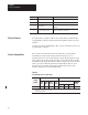
Summary of Changes Summary of Changes Summary of Changes This release of this publication contains new and revised information from the last release. New Information This manual covers the series B version of the 1771-IL isolated input module. The 1771-IL series B module has 16-bit resolution, improved sample time, and auto-calibration. Revised Information Many areas in this manual have been modified.
Preface Using This Manual Purpose of Manual This manual shows you how to use your Isolated Analog Input module with an Allen-Bradley programmable controller. It helps you install, program, calibrate, and troubleshoot your module. Audience You must be able to program and operate an Allen-Bradley programmable controller to make efficient use of your input module. In particular, you must know how to program block transfers. We assume that you know how to do this in this manual.
Preface Using This Manual Appendix Related Products Title Topics Covered A Specifications B Configuration Example C Data Formats D Block transfer with Mini-PLC-2 How to use GET-GET instructions and PLC-2/20 processors Information on BCD, 2s complement binary, signed magnitude You can install your input module in any system that uses Allen-Bradley programmable controllers with block transfer capability and the 1771 I/O structure.
Preface Using This Manual You can place your input module in any I/O module slot of the I/O chassis. You can put two input modules in the same module group. You can put an input and an output module in the same module group. Do not put the module in the same module group as a discrete high density module unless using 1- or 2-slot addressing. Avoid placing output modules close to ac modules or high voltage dc modules.
Table of Contents Overview of the Input Module Chapter 1 Installing the Input Module Chapter 2 Chapter Objectives . . . . . . . . . . . . . . . . . . . . . . . . . . . . . . . . . . . . . . . . . Module Descriptions . . . . . . . . . . . . . . . . . . . . . . . . . . . . . . . . . . . . . . . . Features . . . . . . . . . . . . . . . . . . . . . . . . . . . . . . . . . . . . . . . . . . . . . . . . . . How Analog Modules Communicate with Programmable Controllers . Accuracy . . . . . . . . . . . . . . .
Table of Contents Module Status and Input Data Chapter 5 Calibrating Your Module Chapter 6 Chapter Objectives . . . . . . . . . . . . . . . . . . . . . . . . . . . . . . . . . . . . . . . . . 5-1 Reading Data From Your Module . . . . . . . . . . . . . . . . . . . . . . . . . . . . . . 5-1 Chapter Summary . . . . . . . . . . . . . . . . . . . . . . . . . . . . . . . . . . . . . . . . . . 5-3 Chapter Objective . . . . . . . . . . . . . . . . . . . . . . . . . . . . . . . . . . . . . . . . . .
Chapter 1 Overview of the Input Module Chapter Objectives This chapter gives you information on: features of the module how the input module communicates with programmable controllers Module Descriptions The input module is an intelligent block transfer module that interfaces analog input signals with any Allen-Bradley programmable controllers that have block transfer capability.
Chapter 1 Overview of the Input Module Table 1.A Program Selectable Input Ranges Voltage Ranges Current Ranges 1 to 5V dc 4 to 20mA 0 to 5V dc 0 to 20mA -5 to +5V dc -20 to +20mA -10 to +10V dc 0 to 10V dc How Analog Modules Communicate with Programmable Controllers The processor transfers data to the module (block transfer write, BTW) and from the module (block transfer read, BTR) using BTW and BTR instructions in your ladder diagram program.
Chapter 1 Overview of the Input Module 3. The module converts analog signals into binary or BCD format, and stores these values until the processor requests their transfer. 4. When instructed by your ladder program, the processor performs a read block transfer of the values and stores them in a data table. 5. The processor and module determine that the transfer was made without error, and that input values are within specified range. 6.
Chapter 2 Installing the Input Module Chapter Objectives This chapter gives you information on: calculating the chassis power requirement choosing the module’s location in the I/O chassis configuring your module voltage/current selection jumpers keying a chassis slot for your module wiring the input module’s field wiring arm installing the input module Before You Install Your Input Module Before installing your input module in the I/O chassis you should: You need to: As described under: Calculate th
Chapter 2 Installing the Input Module Power Requirements Your module receives its power through the 1771 I/O power supply. The Isolated Analog input module requires 1.2A at 5V from the power supply. Add this current to the requirements of all other modules in the I/O chassis to prevent overloading the chassis backplane and/or backplane power supply. Module Location in the I/O Chassis Place your module in any I/O module slot of the I/O chassis except for the extreme left slot.
Chapter 2 Installing the Input Module Figure 2.1 Configuration Jumper Settings for 1771-IL/B Inputs Voltage/Current Jumper Functional Analog Block Channel 1 Channel 2 Channel 3 Channel 4 Channel 5 Jumper in Jumper in Current position. Voltage position.
Chapter 2 Installing the Input Module Installing the Analog Module To install your module in an I/O chassis: 1. First, turn off power to the I/O chassis: ATTENTION: Remove power from the 1771 I/O chassis backplane and disconnect the cable from the module before removing or installing an I/O module. Failure to remove power from the backplane could cause injury or equipment damage due to possible unexpected operation.
Chapter 2 Installing the Input Module Figure 2.2 Keying Positions I/O chassis Keying Bands Keying Band Location Between 10 and 12 Between 32 and 34 ATTENTION: Insert or remove keying bands with your fingers. Upper Connector Connecting Wiring to Your Input Module 11022-I 4. Place the module in the plastic tracks on the top and bottom of the slot that guides the module into position. 5. Do not force the module into its backplane connector.
Chapter 2 Installing the Input Module Figure 2.3 Wiring Connections for the Isolated Analog Input Module (1771-IL/B) + 17 18 Analog Source – 15 16 Ground 14 13 + 9 10 11 12 Analog Source – Ground 18 17 Channel 1 16 15 Channel 2 14 Channel 3 13 12 11 10 9 8 7 Channel 4 Channel 5 6 5 Channel 6 4 3 Channel 7 7 8 5 6 3 4 2 2 1 1 Channel 8 NOTE: The 1771-IL/B module does not supply loop power for loop powered analog sources (transmitters, transducers, etc.).
Chapter 2 Installing the Input Module Grounding When using shielded cable wire, ground the foil shield and drain wire only at one end of the cable. We recommend that you wrap the foil shield and drain wire together and connect them to a chassis mounting bolt (Figure 2.4). At the opposite end of the cable, tape exposed shield and drain wire with electrical tape to insulate it from electrical contact. Figure 2.4 Cable Grounding Remove a length of cable jacket from the Belden 8761 cable.
Chapter 2 Installing the Input Module Indicator Lights The front panel of the input module contains a green RUN and a red FLT (fault) indicator (Figure 2.5). At powerup, an initial module self-check occurs. If there is no fault, the red indicator turns off. The green indicator will blink until the processor completes a successful write block transfer to the module. Upon completion of a block transfer write (BTW), the green RUN indicator will be on and the red FLT indicator will be off.
Chapter 3 Communicating With Your Module Chapter Objectives In this chapter, we describe block transfer programming quick-start sample programs in the PLC-2, PLC-3 and PLC-5 processors module scan time issues Block Transfer Programming Your module communicates with your processor through bidirectional block transfers. This is the sequential operation of both block transfer read (BTR) and block transfer write (BTW) instructions.
Chapter 3 Communicating With Your Module PLC-2 Programming The PLC-2 program example regulates when each block transfer will be initiated to eliminate problems caused by limited regulation of bidirectional block transfers. Both storage bits are needed, (as shown in the example), to accomplish this task in all PLC-2 systems, local or remote, with long or short program scans. Therefore, the program as shown is the minimum required.
Chapter 3 Communicating With Your Module PLC-3 Programming Block transfer instructions with the PLC-3 processor use one binary file in a data table section for module location and other related data. This is the block transfer control file. The block transfer data file stores data that you want transferred to your module (when programming a block transfer write) or from your module (when programming a block transfer read).
Chapter 3 Communicating With Your Module PLC-5 Programming The PLC-5 program is very similar to the PLC-3 program with the following exceptions: 1. Block transfer enable bits are used instead of done bits as the conditions on each rung. 2. Separate block transfer control files are used for the block transfer instructions. Figure 3.
Chapter 3 Communicating With Your Module Module Scan Time Scan time is defined as the amount of time it takes for the input module to read the input channels and place new data into the data buffer. Scan time for your module is shown in Appendix A. Figure 3.4 Block Transfer Time Module available to perform block transfer End of Block Transfer Write Block Transfer Write Time 1 Configure Time 1st Scan 2 3 2nd Scan 4 5 3rd Scan 6 10529-I Internal Scan time = 50ms T = 100ms, 200ms, 300ms, 3.1s.
Chapter 4 Configuring Your Module Chapter Objectives In this chapter you will read how to: configure your module’s hardware condition your inputs enter your configuration data. Configuring Your Input Module Because of the many analog devices available and the wide variety of possible configurations, you must configure your module to conform to the analog device and specific application that you have chosen.
Chapter 4 Module Configuration During normal operation, the processor transfers from 1 to 37 words to the module when you program a BTW instruction to the module’s address. The BTW file contains configuration words, high and low channel alarm settings, and calibration values for each channel. When a block transfer write length of 0 is programmed, the 1771-IL series B will respond with the Series A default length of 19.
Chapter 4 Module Configuration Table 4.B Input Voltage and Current Ranges for the Analog Input Module Nominal Voltage or Current Range Default Scaling BCD Output Range Voltage or Current Per Bit Data from A/D Converter Voltage or Current Per Bit +1 to +5V 0000 to +4095 0.98mV 3063 to 15316 0.33mV 0 to 5V 0000 to +4095 1.22 mV 32768 to 15316 0.33mV -5 to +5V -4095 to +4095 1.22mV -15316 to 15316 0.33mV -10 to +10V -4095 to +4095 2.44mV -30632 to 30632 0.
Chapter 4 Module Configuration Data Format You must also indicate what format will be used to read data from your module. Typically, BCD is selected with PLC-2 processors, and 2’s complement binary is selected with PLC-3 and PLC-5 processors. See Appendix C for details on data format. Table 4.
Chapter 4 Module Configuration Figure 4.2 Digital Filter Lag Equation Illustration 100% 63% Amplitude 0 Unfiltered Input TA = 0.01 sec TA = 0.5 sec TA = 0.99 sec 0 0.01 0.5 0.99 Time in Seconds 16723 Digital filter time constant values of .00 BCD to .99 BCD (0.00 to 2.55 binary) (.00 = no filter) are set in bits 00 through 07 of word 3 of the block transfer write instruction. If an invalid digital filter value is entered (i.e., .
Chapter 4 Module Configuration Set appropriate bits in the BTW data file to enable the RTS mode. You can select RTS periods ranging from 50 ms to 3.1 seconds in increments of 100ms for the 1771-IL/B. Refer to Table 4.E below for actual bit settings. Note that the default mode of operation is implemented by placing all zeroes in bits 11 through 15 (13 through 17 octal). Table 4.
Chapter 4 Module Configuration Scaling Each channel has two scaling points, low and high. The signal value at these points is fixed. For example, the high scaling point of a +10V output channel always corresponds to an input signal equal to +10.000V. To implement the scaling feature, you insert the minimum and maximum scaled values in the appropriate configuration words. The format of the scaling values is determined by the BTW format bit (bit 08, word 2). The range in BCD format is +9999.
Chapter 4 Module Configuration Scaling Ranges The maximum range of the scaling values is +9999 BCD or +32767 binary. These values must be entered in the format selected in word 2, bit 08 (10). If invalid values are entered into the scaling words, the corresponding input in the BTR data will be zero and the invalid scaling bit will be set. Table 4.
Chapter 4 Module Configuration Alarms Each input channel has alarm functions that provide status indication through associated status bits in the block transfer read data returned by the module. Underrange alarm - This bit is set if the input falls below the minimum range for that specific input type. This alarm is predefined and cannot be changed by the user. In current loop inputs, this bit also indicates an open loop.
Chapter 4 Module Configuration Default Configuration If a write block with all zeroes is written to the module, the default selections will be: 1 to 5V dc or 4 to 20mA (depends on voltage/current selection jumper) BCD data format no real time sampling (RTS) no digital filter no scaling no alarms Note: Input data is set to 0 until an initial block transfer write is received by the module. Figure 4.
Chapter 4 Module Configuration Decimal Bits 15 14 13 12 11 10 09 08 07 06 05 04 03 02 01 00 Octal Bits 17 16 15 14 13 12 11 10 07 06 05 04 03 02 01 00 6 5 4 3 2 1 G O 17 Channel 7 - maximum scaling 18 Channel 8 - minimum scaling 19 Channel 8 - maximum scaling 8 7 6 5 4 3 2 1 8 7 2 20 Sign bits, low alarm values Sign bits, high alarm values 21 Channel 1 - Low Alarm Value 22 Channel 1 - High Alarm Value 23 Channel 2 - Low Alarm Value 24 Channel
Chapter 4 Module Configuration Bit/Word Descriptions for the Isolated Analog Input Module Configuration Block Note that decimal bits are shown. Octal bits are shown in parentheses. Word Decimal Bit (Octal Bit) Description Word 1 Bits 00-15 (00-17) Input range selections, grouped 2 bits for each channel, allow selection of any of 7 input voltage or current ranges. See Table 4.A. Bits 00-07 Digital filter reduces effect of noise on the input. See “Digital Filtering.” Bit 08 (10) BTW format bit.
Chapter 4 Module Configuration Word Decimal Bit (Octal Bit) Description Bit 00 Offset Calibration bit. When this bit is set (1), offset calibration is to be performed. When set, no other calibration function bits can be set. Default is 0, no offset calibration. Bit 01 Gain Calibration bit. When this bit is set (1), gain calibration is to be performed. When set, no other calibration function bits can be set. Default is 0, no gain calibration. Bit 02 Save calibration values.
Chapter 5 Module Status and Input Data Chapter Objectives In this chapter you will read about: reading data from your module block transfer read data format Reading Data From Your Module Block transfer read programming moves status and data from the input module to the processor’s data table in one I/O scan (Figure 5.1). The processor’s user program initiates the request to transfer data from the input module to the processor. Figure 5.
Chapter 5 Module Status and Input Data The Isolated Analog Input Module (1771-IL series B) reports the status of all eight channels to the processor as outlined below. Table 5.A Bit/Word Descriptions for the Isolated Analog Input Modules (1771-IL) Read Block Transfer Data Word Decimal Bit (Octal Bit) Description Bit 00 Power up bit (PU) is set after initial power up. It will not reset until the module receives a valid write block transfer.
Chapter 5 Module Status and Input Data Word Decimal Bit (Octal Bit) Description Bits 00-07 (00-07) Low Alarm bits for channels 1 through 8 respectively. Each bit represents an alarm indicator for that channel. When the bit is set, the value of that channel is below the low alarm value. Bits 08-15 (10-17) Not used Bits 00-07 (00-07) High Alarm bits for channels 1 through 8 respectively. Each bit represents an alarm indicator for that channel.
Chapter 6 Module Calibration Chapter Objective In this chapter we tell you how to calibrate your module. Tools and Equipment To calibrate your input module you will need the following tools and equipment: Tool or Equipment Description Model/Type Precision Voltage Source 0-10V, 1µV resolution; Accuracy of better than 2mV Analogic 3100, Data Precision 8200 or equivalent Industrial Terminal and Interconnect Cable Programming terminal for A-B family processors Cat. No. 1770-T3 or Cat. No.
Chapter 6 Module Calibration Performing Auto-calibration Calibration of the module consists of applying 0.00000V across each input channel for offset calibration, and +10.00000V across each input channel for gain correction. ATTENTION: Verify that each channel’s configuration jumper is set to the voltage mode (refer to “Setting the Voltage/Current Selection Jumpers” in chapter 2.) Failure to do so can damage the module. Offset Calibration Normally all inputs are calibrated together.
Chapter 6 Module Calibration 4. After the connections stabilize, request the offset calibration by setting bit 00 in block transfer write word 37 and sending a block transfer write (BTW) to the module. Refer to Table 6.A. When the BTW is sent, all channels are calibrated to 0.00000V. Table 6.
Chapter 6 Module Calibration Gain Calibration Calibrating gain requires that you apply +10.00000V across each input channel. To calibrate the gain of an input, proceed as follows: NOTE: Normally, all channels are calibrated simultaneously (decimal bits 08015, octal bits 10-17 of word 37 are 0). To disable calibration on any channel, set (1) the corresponding bit 08-15 decimal (10-17 octal) of word 37. 1. Apply +10.00000V across each input channel as shown in Figure 6.2. Figure 6.2 Applying 10.
Chapter 6 Module Calibration Save Calibration Values If any ”uncalibrated channel” bits 08-15 (10-17 octal) of word 15 are set, a save cannot occur. Auto-calibration should be performed again, starting with offset calibration. If the module has a faulty channel, the remaining functioning channels can be calibrated by inhibiting calibration on the faulty channel. The module can be run with the new calibration values, but will lose them on power down.
Chapter 7 Troubleshooting Chapter Objective We describe how to troubleshoot your module by observing indicators and by monitoring status bits reported to the processor.
Chapter 7 Troubleshooting Troubleshooting with the Indicators Table 7.A shows indications, probable causes and recommended actions to correct common faults. Table 7.A Troubleshooting Chart for the Isolated Analog Input Module (1771-IL series B) Indication Probable Cause No power to module RUN FLT B RUN and FLTT are OFF Both Recommended Action Check power to I/O chassis. Recycle as necessary. Possible short on the module LED driver failure Replace module..
Chapter 7 Troubleshooting Table 7.B Status Reported in Word 1 Word Word 1 Decimal Bit (Octal Bit) Description Bit 00 Power up bit (PU) is set after initial power up. It will not reset until the module receives a valid write block transfer. Note: Input data is set to zero until the first BTW is received. Bit 01 Out of range bit (OR) is set if one or more channels are either over or under range. Bit 02 Invalid scaling bit (IS) is set if the firmware cannot use the scaling data in the BTW.
Chapter 7 Troubleshooting Status Reported in Words 13 and 14 Design your program to monitor over/under alarm bits, and to take appropriate action depending on your application requirements. You may also want to monitor these bits while troubleshooting with your industrial terminal. Bits 00-07 each represent an input for channels 1-8, respectively. For example, bit 04 represents input channel 5. The module sets a bit (1) to indicate it has detected an alarm condition. Refer to Table 7.D. Table 7.
Chapter 7 Troubleshooting Status Reported in Word 15 Design your program to monitor status bits in word 15 during auto-calibration, and to take appropriate action depending on your requirements. You may also want to monitor these bits while troubleshooting with your industrial terminal. The module sets a bit (1) to indicate it has detected one or more of the following conditions as shown in Table 7.E. Table 7.
Appendix A Specifications Inputs per module 8 fully isolated differential Module Location 1771 I/O rack - 1 slot Input voltage ranges (nominal) +1 to +5V DC 0 to 5V DC -5 to +5V DC -10 to +10V DC Input current ranges (nominal) +4 to +20mA 0 to +20mA -20 to +20mA Resolution 16-bit binary over full range Accuracy Voltage: Current: Typical - 0.01% of full scale range @ 25oC Maximum - 0.05% of full scale range @ 25oC Typical - 0.06% of full scale range @ 25oC Maximum - 0.
Appendix A Specifications Specifications continued Calibration Interval calibration should be checked at 6 month intervals to maintain specified accuracy Internal scan rate 50 milliseconds for 8 channels Environmental conditions operational temperature: storage temperature: relative humidity Conductors Wiring Category 0 to 600C (32 to 1400F) -40 to 850C (-40 to 1850F Operating: 5 to 95% (without condensation) Non-operating: 5 to 80% (without condensation) 14 gauge stranded (max.
Appendix B Configuration Example Sample Configuration of the Analog Input Module The following is a sample configuration for the 1771-IL series B isolated analog input module. Entering the data shown in Figure B.1 in the configuration words of the write block transfer data file will result in the following module setup. Overall Module Functions Chosen Digital Filter Time Constant 0.5 seconds Data Format 2’s Complement Binary Real Time Sampling Rate 1.
Appendix B Configuration Example Figure B.1 Sample PLC-5 Data File (Hexadecimal Data) for an Isolated Analog Input Module (cat. no.
Appendix C Data Table Formats 4-Digit Binary Coded Decimal (BCD) The 4-digit BCD format uses an arrangement of 16 binary digits to represent a 4-digit decimal number from 0000 to 9999 (figure C.1). The BCD format is used when the input values are to be displayed for operator viewing. Each group of four binary digits is used to represent a number from 0 to 9. The place values for each group of digits are 20, 21, 22 and 23 (Table C.A).
Appendix C Data Formats Table C.A BCD Representation Signed-magnitude Binary 23 (8) Place Value 22 (4) 21 (2) 20 (1) Decimal Equivalent 0 0 0 0 0 0 0 0 1 1 0 0 1 0 2 0 0 1 1 3 0 1 0 0 4 0 1 0 1 5 0 1 1 0 6 0 1 1 1 7 1 0 0 0 8 1 0 0 1 9 Signed-magnitude binary is a means of communicating numbers to your processsor. It should be used with the PLC-2 family when performing computations in the processor.
Appendix C Data Formats First, the two’s complement method places an extra bit (sign bit) in the left-most position, and lets this bit determine whether the number is positive or negative. The number is positive if the sign bit is 0 and negative if the sign bit is 1. Using the complement method: 0 10110 = 22 To get the negative using the two’s complement method, you must invert each bit from right to left after the first “1” is detected.
Appendix D Block Transfer (Mini-PLC-2 and PLC-2/20 Processors) Multiple GET Instructions Mini-PLC-2 and PLC-2/20 Processors Programming multiple GET instructions is similar to block format instructions programmed for other PLC-2 family processors. The data table maps are identical, and the way information is addressed and stored in processor memory is the same. The only difference is in how you set up block transfer read instructions in your program.
Appendix D Block Transfer (Mini–PLC–2 and PLC–2/20 Processors) Rungs 2 and 3: These output energize instructions (012/01 and 012/02) define the number of words to be transferred. This is accomplished by setting a binary bit pattern in the module’s output image table control byte. The binary bit pattern used (bits 01 and 02 energized) is equivalent to 6 words or channels, and is expressed as 110 in binary notation.
Appendix D Block Transfer (Mini–PLC–2 and PLC–2/20 Processors) Setting the Block Length (Multiple GET Instructions only) The input module transfers a specific number of words in one block length. The number of words transferred is determined by the block length entered in the output image table control byte corresponding to the module’s address. The bits in the output image table control byte (bits 00-05) must be programmed to specify a binary value equal to the number of words to be transferred.
Index A alarms, 4-9 overrange, 4-9 underrange, 4-9 F features, 1-1 field wiring arm, 2-5 filtering, 4-4 B BCD format, 1-3 bit settings, voltage or current input, 4-2 block transfer, 1-1, 2-2, 3-1 write, 4-5 block transfer read, 3-1, 3-2, 5-1 word assignments, 5-1 block transfer write, 3-2 BTR format, bit/word descriptions, 5-2 G grounding, 2-7 C Calibration, tools, 6-1 communication, 1-2 configuration, default, 4-10 configuration block, 4-10 bit/word descriptions, 4-12 configuration BTW, 3-1 configurin
Index S scaling implementation, 4-7 ranges, 4-8 scan time, 3-5 specifications, A-1 U update time, 1-1 W wiring connections, 2-6 T Troubleshooting, table, 7-2 PLC is a registered trademark of Allen-Bradley Company, Inc. PLC-5 is a trademark of Allen-Bradley Company, Inc. SLC is a trademark of Allen-Bradley Company, Inc.
Allen-Bradley has been helping its customers improve productivity and quality for 90 years. A-B designs, manufactures and supports a broad range of control and automation products worldwide. They include logic processors, power and motion control devices, man-machine interfaces and sensors. Allen-Bradley is a subsidiary of Rockwell International, one of the world’s leading technology companies. With major offices worldwide.