Because of the variety of uses for the products described in this publication, those responsible for the application and use of this control equipment must satisfy themselves that all necessary steps have been taken to assure that each application and use meets all performance and safety requirements, including any applicable laws, regulations, codes and standards. The illustrations, charts, sample programs and layout examples shown in this guide are intended solely for example.
This manual shows you how to use your Fast Analog Input module with an Allen-Bradley programmable controller. It helps you install, program, calibrate, and troubleshoot your module. You must be able to program and operate an Allen-Bradley programmable controller to make efficient use of your input module. In particular, you must know how to program block transfers. We assume that you know how to do this in this manual.
P2–2 Using This Manual - )+' -, (!)+' -$)( )( , )'*& ' (- $( +0 ,$"( ' "($-. 1 $- $( +0 &) % -+ (,! + /$-# $($1 1 ( 1 *+) ,,)+, )/ -) ., 1 $(,-+. -$)(, )+', , !.& !)+', !)+ $ (-$!0$(" 0).+ - - & We use these conventions in this manual: -# - -# + $, ')+ $(!)+' -$)( ).- -)*$ $( ()-# + # *- + $( -#$, ' (. & -# - -# + $, ')+ $(!)+' -$)( ).
Using This Manual ! $ # # #% P2–3 The 1771-IFF series A module can be used with any 1771 I/O chassis. Communication between the discrete analog module and the processor is bidirectional; the processor block-transfers output data through the output image table to the module and block-transfers input data from the module through the input image table. The module also requires an area in the data table to store the read block transfer data and write block transfer data.
P2–4 Using This Manual
Table of Contents )"15&3 #+&$5*7&4 0%6-& &4$3*15*0/ &"563&4 30(3". &-&$5"#-& /165 "/(&4 08 /"-0( 0%6-&4 0..6/*$"5& 8*5) 30(3"..
Table of Contents *#26'4 $,'%6+8'5 10(+)74+0) "174 0276 1&7.' 0276 #0)' '.'%6+10 0276 #0)' '.'%6+10 +65 0276 1.6#)' #0& 744'06 #0)'5 (14 6*' #56 0#.1) 0276 1&7.
iii Table of Contents Troubleshooting Your Input Module Specifications Chapter 7 Chapter Objective . . . . . . . . . . . . . . . . . . . . . . . . . . . . . . . . . . . . Diagnostics Reported by the Module . . . . . . . . . . . . . . . . . . . . . . . Diagnostic Bits Reported By the Analog Input Module . . . . . . . . . Troubleshooting Chart for the Fast Analog Input Module (1771ĆIFF/A) . . . . . . . . . . . . . . . . . . . . . . . . CheckingModule Operation . . . . . . . . . . . . . . . . . . . . . . .
Table of Contents
! ! # In this chapter, we describe: • checking your calibration • calibrating your module. $ ! ! " "! " Your module is shipped to you already calibrated. If you are checking calibration, or if it becomes necessary to recalibrate the module, you must do so with the module in an I/O chassis. The module must communicate with the processor and industrial terminal.
1–2 Calibrating Your Module If a calibration check of your module becomes necessary: 1. Verify that the module is in voltage mode. In single-ended mode, apply voltages to channels 1 through 16. 2. Send a configuration block transfer write to the module that replicates the specific application. (This forces the module to do an internal calibration.) 3. Apply –10V, –5V, –2.5V 0V, 1V, 2.5V, 5V, and 10V to the module.
Calibrating Your Module Calibrating your Input Module 1–3 The fast analog input module is shipped already calibrated. Calibration of the module consists of applying a voltage or current across each input channel for offset and gain calibration. Offset and gain values are shown in the following table. Table 1.
1–4 Calibrating Your Module The BTR echoes back the status of each of the channels to verify calibration. If selected channels were calibrated satisfactorily, the BTR will reflect this by having their bits set to 1. (In Differential mode, the upper byte of word 21 in the BTR is not set (bits 8–15 decimal or 10–17 octal are 0).
Calibrating Your Module 1–5 The BTR echoes back the status of each of the channels to verify the calibration. If all channels were calibrated satisfactorily, the BTW will reflect this by having all bits set to 1.
1–6 Calibrating Your Module
In this chapter, we describe how to troubleshoot your fast analog module by: • • • • • observing the indicators monitoring status bits reported to the processor.
2–2 Troubleshooting Your Input Module An invalid scaling data bit (bit 02) is set if invalid scaling data is entered into any of the minimum/maximum scaling value words. Note that minimum equal to maximum is an invalid value. If invalid values are entered into the minimum or maximum scaling words the corresponding read block transfer input channel word will be set to 0000. Bit 02 is set if an invalid digital filter value is entered (e.g., 1F).
Troubleshooting Your Input Module 2–3 The following table lists the probable cause and recommended actions for some common trouble indications. ! ! "" ) '%)&%)# ! ! " #,!!) ,! *,( ' *+!, .%*) *)! '%)&%)# *"" 1 %.%)# *)"%#/, .%*) '* & , )-"!, ,%.! !) *)"%#/, .%*) #,!!) ,! , 1 ,! " %'/,! %) (* /'! !.
2–4 Troubleshooting Your Input Module The following allows you to run a check on module operation, and isolate a fault either to the module or external to the module. Set up a 1771 I/O chassis with a PLC-5 processor in the leftmost slot. Set the chassis backplane switch 5 to ON. All other backplane switches to Off. This sets the chassis to 1Ćslot addressing.
Troubleshooting Your Input Module 2–5 Enter the following ladder logic into the processor. BT9:0 BT9:1 EN EN 1 Note: This programming is only to test the block transfer write and read functions. It is not intended for regular use.
2–6 Troubleshooting Your Input Module The module also reports status and specific faults (if they occur) in every transfer of data (BTR) to the PC processor. Monitor the green and red indicators and the status bits in word 1 of the BTR file when troubleshooting your module.
Troubleshooting Your Input Module 2–7 After determining that the module is operating correctly, troubleshoot any faulty inputs by: • measuring each input with respect to module common • disconnecting inputs from the field wiring arm one at a time while observing module action • testing for input channel functionality During this procedure, monitor the input data table of the programmable controller and observe any changes which occu
2–8 Troubleshooting Your Input Module 5. Attempt to equalize all grounds at the offending channel before reconnecting the input wiring. ! ATTENTION: Remove power from the 1771 I/O chassis backplane and field wiring arm before removing or installing input wiring. • Failure to remove power from the backplane or wiring arm could cause module damage, degradation of performance, or injury.
Troubleshooting Your Input Module 2–9 To test the functionality of an input channel: 1. Remove the input wiring from the field wiring arm. ! ATTENTION: Remove power from the 1771 I/O chassis backplane and field wiring arm before removing or installing input wiring. • Failure to remove power from the backplane or wiring arm could cause module damage, degradation of performance, or injury.
2–10 Troubleshooting Your Input Module
Overview of the Fast Analog Input Module This chapter, we describe: • features of the module • how the module communicates with programmable controllers The fast analog input module is an intelligent block transfer module that interfaces analog input signals with any Allen-Bradley programmable controllers that have block transfer capability.
3–2 Overview of the Fast Analog Input Module &" &" &" &" ) &" ) &" ) &" &" The processor transfers data to the module (block transfer write) and from the module (block transfer read) using BTW and BTR instructions in your ladder diagram program.
Overview of the Fast Analog Input Module 3–3 3. The module converts analog signals into binary or BCD format, and stores theses values until the processor requests their transfer. 4. When instructed by your ladder program, the processor performs a read block transfer of the values and stores them in a data table. 5. The processor and module determine that the transfer was made without error, and that input values are within specified range. 6.
3–4 Overview of the Fast Analog Input Module
Installing the Input Module In this chapter, we tell you about: • • • • • • calculating the chassis power requirement choosing the module’s location in the I/O chassis configuring your module configuration plugs keying a chassis slot for your module installing the input module wiring the input module’s field wiring arm If this product has the CE mark it is approved for installation within the European Union and EEA regions.
Before installing your input module in the I/O chassis: % .% - -" )(/ + + *.#+ & '-, ( %% &( .% , #' " " ,,#, (/ + *.#+ & '-, ) ! - +&#' /" + -( )% -" &( .% #' -" " ,,#, ( .% ( -#(' #' -" " ,,#, ) ! 0 -" $)% ' ('' -(+ #' -" " ,,#, ( .% 0#'! ) ! $ ('' -#(', -( -" /#+#'! +& #+#'! (.+ ').- ( .% ) ! ' +(.
Place your module in any I/O module slot of the I/O chassis except for the extreme left slot. This slot is reserved for PC processors or adapter modules. Group your modules to minimize adverse affects from radiated electrical noise and heat. We recommend the following. • Group analog input and low voltage dc modules away from ac modules or high voltage dc modules to minimize electrical noise interference.
&%) * %$ * %$ +( * %$ &"+ ) ))% * - * $&+* $$ " %( $ *% /%+( ( '+ ( # $*) %+ $ # . ,%"* #% $ +(( $* #% ) ** $ ) %$ * #% +" ! )+( * * * $* ( #% +" ) ) * %( * ( ) $ " 0 $ %( ( $* " % $%* # .
Place your module in any slot in the chassis except the leftmost slot which is reserved for processors or adapters. ! ATTENTION: Observe the following precautions when inserting or removing keys: • insert or remove keys with your fingers • make sure that key placement is correct Incorrect keying or the use of a tool can result in damage to the backplane connector and possible system faults.
To install your module in an I/O chassis: 1. First, turn off power to the I/O chassis: ATTENTION: Remove power from the 1771 I/O chassis backplane and field wiring arm before removing or installing an I/O module. ! • Failure to remove power from the backplane or wiring arm could cause module damage, degradation of performance, or injury. • Failure to remove power from the backplane could cause injury or equipment damage due to possible unexpected operation.
Connect your I/O devices to the cat. no. 1771-WG wiring arm shipped with the module. The wiring arm is attached to the pivot bar at the bottom of the I/O chassis. It pivots upward and connects with the module so you can install or remove the module without disconnecting the wires. ! ATTENTION: Remove power from the 1771 I/O chassis backplane and field wiring arm before removing or installing an I/O module.
" ! " Channel 1 Refer to transmitter manufacturers specifications for power supply connections. 2Channel Power Supply 2ĆWire Transmitter Power Supply 2 3 3 Channel 4 + 2ĆWire Transmitter 1 Channel 2 1Module - Common Channel 5 7 Channel 7 8 Channel 8 1Module Common Channel 9 together inside the module. Source Ground 2 Jumper all unused channels to module common to reduce noise.
! " ! ! " Channel 1 Refer to transmitter manufacturers specifications for power supply connections. Power Supply Power Supply 4ĆWire Transmitter 4ĆWire Transmitter Channel 2 2Channel 3 Channel 4 + 1Module - Common Channel 5 Channel 6 + Channel 7 - Channel 8 1Module Common Channel 9 Channel 10 Source Ground 1 All commons are electrically tied together inside the module.
" ! ! "! # $ !! Channel 1+ ! Refer to transmitter manufacturers specifications for power supply connections. 2ĆWire Transmitter Power Supply 2ĆWire Transmitter 2 Channel 2+ + Channel 2Ć - Not used 3 4 5 Channel 3+ 6 Channel 3Ć + Power Supply 1 Channel 1Ć 7 Channel 4+ - 8 Channel 4Ć 9 Not used 10 Channel 5+ 11 Channel 5Ć 1.
! Channel 1+ Power Supply 4ĆWire Transmitter 1 Channel 1Ć Refer to transmitter manufacturers specifications for power supply connections.
When using shielded cable wire, ground the foil shield and drain wire only at one end of the cable. We recommend that you wrap the foil shield and drain wire together, and connect them to a chassis mounting bolt, grounding stud or chassis single-point grounding point (Figure 4.5). Use heat shrink tubing to seal the exit point of the wires. At the opposite end of the cable, tape exposed shield and drain wire with electrical tape to insulate it from electrical contact.
The front panel of the fast analog input module contains a green RUN indicator and a red FAULT indicator. At power-up an initial module self-check occurs. If there is no fault, the red indicator turns off. % # !# ! &$% !# ! &$% ( The green indicator comes on when the module is powered. It will flash until the module is programmed. If a fault is found initially or occurs later, the red fault indicator lights.
In this chapter we describe: • block transfer programming • sample programs in the PLC-2, PLC-3 and PLC-5 processors • module scan time issues Your module communicates with your processor through bidirectional block transfers. This is the sequential operation of both read and write block transfer instructions.
Module Programming ! The PLC-2 program example regulates when each block transfer will be initiated to eliminate problems caused by limited regulation of bidirectional block transfers. Both storage bits are needed, as shown in the example, to accomplish this task in all PLC-2 systems, local or remote, with long or short program scans. Therefore, the program as shown is the minimum required.
Module Programming Block transfer instructions with the PLC-3 processor use one binary file in a data table section for module location and other related data. This is the block transfer control file. The block transfer data file stores data that you want transferred to your module (when programming a block transfer write) or from your module (when programming a block transfer read). The address of the block transfer data files are stored in the block transfer control file.
Module Programming The PLC-5 program is very similar to the PLC-3 program with the following exceptions: 1. You must use enable bits instead of done bits as the conditions on each rung. 2. A separate control file must be selected for each of the block transfer instructions. Refer to Appendix B. 7 329)5<83 7,) 352+5%0 )1%&/)6 % &/2'.
Module Programming Module Scan Time 5-5 Scan time is defined as the amount of time it takes for the input module to read the input channels and place new data into the data buffer. Word 24 of the block transfer write data table shows the scan time for the module for the given configuration. These figures are the time it takes to sample all channels and process the data. Refer to Appendix A for tables showing common scan times at various oversample rates. Table 10.
Module Programming The following description references the sequence numbers in Figure 5.4. Following a block transfer write “1” the module inhibits communication until after it has configured the data “2,” performed calibration check “3” (if requested), scanned the inputs “4,” and filled the data buffer “5.” Write block transfers, therefore, should only be performed when the module is being configured or calibrated. Any time after the second scan begins “6,” a BTR request “7” can be acknowledged.
In this chapter, we describe; • configuring your module’s features • conditioning your inputs • entering your data. Because of the many analog devices available and the wide variety of possible configurations, you must configure your module to conform to the analog device and specific application that you have chosen.
During normal operation the processor transfers 1 to 41 words to the module when you program a block transfer write instruction to the module’s address. This BTW file contains configuration words, and calibration words (words 38 and 39) for each channel. When a block transfer transfer length of 0 is programmed, the 1771-IFF/A will respond with the 1771-IFE series A default length of 37. ! You can configure the module to operate with any of five voltage or three current ranges.
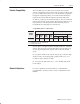
6-3 Input Voltage and Current Ranges for the Fast Analog Input Module Nominal Voltage or Current Range Corresponding 4ĆDigit BCD Output Range Corresponding 12ĆBit Binary Output Range Voltage or Current Per Bit .* .* .* ( .* .* .* ( 3 .* 3 .* 3 .* ( 3 .* 3 .* 3 .* ( .* ( .* .* ( .* ( .* .* ( 3 .
6-4 Two's complement binary, data first In two’s complement binary – data first mode, the channel data will appear in word 1 through 8 (differential) or 1 through 16 (single-ended). Diagnostic and status information which previously appeared in words 1 through 4 will appear after the channel data. Digital Filtering The module has hardware-based high frequency filters on all channels to reduce the effect of electrical noise on the input signal.
The real time sampling (RTS) mode of operation provides data gathered at precisely timed intervals for use by the processor. BTW word 3 bits 11–15 (13–17 octal) are used to set the real time sampling interval. RTS is invaluable for time based functions (such as PID and totalization) in the PLC. It allows accurate time based calculations in local or remote I/O racks.
Your module can perform linear conversion of unscaled data to engineering units, (for example; gallons/minute, degrees C, degrees F and pounds/square inch). Unscaled data in the module has a range of 0 through 4095 for the unipolar ranges (0 to 5V dc/0 to 20mA and 1 to 5V dc/4 to 20mA); and -4095 to +4095 (8190) for the bipolar ranges (+5V/+20mA and +10V). BTW words 6 through 37 are the scaling words for channels 1 through 16.
Scaling values must always be entered in BCD format, even if the data format chosen is binary. If scaling is selected for any channel, all channels must be scaled. If scaling is not required on certain channels, set those to the default input range: 0 to 4095 for 0 to + voltage or current ranges, and -4095 to +4095 for - to + voltage or current ranges. If scaling is not selected, the module requires specific minimum BTR file lengths for the number of channels used.
This feature (oversampling) is set in block transfer word 40. This word specifies the number of times a channel will be sampled and the results averaged. Legal values of the number of oversamples are: 0, 1, 2, 4, 8, 16, 32, 64, 128, and 256. The format of the data in this field can be BCD or binary.
6-9 Default Configuration If a write block of five words, with all zeroes, is sent to the fast analog input module (cat. no. 1771-IFF series A), default selections will be: • 1 to 5V dc or 4 to 20mA (dependent on configuration jumper • • • • • • • setting) BCD data format no real time sampling (RTS) no filtering no scaling single-ended inputs 8 times oversample no disabled channels Table 11.A Fast Analog Input Module (1771ĆIFF/A) Block Transfer Write Configuration Block Dec.
6-10 Bit/Word Descriptions for the Analog Input Module Block Transfer Write Configuration Block Note that decimal bits are shown, with octal bits in parentheses. Word Decimal Bit (Octal Bit) Description Words 1 and 2 Bits 00Ć15 (00Ć17) Input range selections allow the user to configure the inputs for any of 7 input voltage or current ranges. Two bits are required for each channel. Bits 00 and 01 for channel 1, bits 02 and 03 for channel 2, etc.
! ! ! +- +- +- ! %/. 5 5 ! $ %/ -!,-!.!*/. $ **!( %/ /+ $ **!( %/ /+ $ **!( !/ $!* /$! %/ %. .!/ * $ . !!* .!*/ /$! )+ 0(! 2%(( -! /$! $ **!(. * &0./ /$! # %* +--! /%+* 1 (0!. " 0.! +* /+ +- /+ - *#!. 1 (0! +" %. !3,! /! " 0.! +* - *#! %. !3,! /! * %""!-!*/% ( )+ ! %/. /$-0 /$-0 %* + / ( -! %#*+-! * 0--!*/ )+ ! ,,(4 ) %/.
Chapter Objectives In this chapter, we describe: • reading data from your module • block transfer read block format Reading Data From Your Module Block transfer read programming moves status and data from the input module to the processor’s data table in one I/O scan (Figure 7.1). The processor’s user program initiates the request to transfer data from the input module to the processor. Figure 7.
7-2 When a BTR length of 0 is programmed, the 1771-IFF/A will respond with the 1771-IFE series A module default length of 20. Block Transfer Read Format The bit/word description for the block transfer read of the fast analog input module is described below. Table 12.A BTR Word Format for the Fast Analog Input Module Word Word 1 Word 2 Word 3 Word 4 Decimal Bit (Octal Bit) Description Bit 00 Power up bit (PU) - Used by the module to tell the processor that it is alive but not yet configured.
! # # # " ! # *, %.- ! # ! "$ #" #" $ %. ,!+,!-!).- $ ))!' ".!, '% , .%*) $ - !!) -!). .$! (* /'! *)"%,(- '% , .%*) 2 ! $*%)# & .$! $ ))!'- .$ . 1!,! '% , .! /,%)# .$! # %) '% , .%*) ) %""!,!).% ' (* ! $ ))!'- .$,/ ,! 3!,* *, %.- # $%- 1*, %- (- */).!, .* .%(!-. (+ .$! '* & , )-"!, ! */ ) -/ ., . .$! .%(! -. (+ *" ",*( )*.$!, .* "%) .
7-4 Data First Configuration When bits 9 and 10 in block transfer write word 3 are set for “two’s complement – data first configuration,” the block transfer read will have the channel data first in the transfer. Figure 7.2 Block Transfer Read in Two's Complement - Data First Configuration, SingleĆended Inputs Dec.
7-5 Figure 7.3 Block Transfer Read in Two's Complement - Data First Configuration, Differential Inputs Dec.
Inputs per module Module Location 16 single-ended; 8 differential low level 1771 I/O rack - 1 slot +1 to +5V dc 0 to +5V dc -5 to +5V dc -10 to +10V dc 0 to +10V dc Input voltage ranges (nominal) +4 to +20mA 0 to +20mA -20 to +20mA Input current ranges (nominal) Resolution Accuracy Linearity Repeatability Isolation Voltage Input overvoltage protection Input overcurrent protection (current ranges) Common mode voltage Input impedance Common mode rejection Curr
A-2 Description Value between 10 and 12 between 24 and 26 Catalog Number 1771-WG 7Ć9 inchĆpounds • CSA certified • CSA Class I, Division 2, Groups A, B, C, D certified • UL listed • CE marked for all applicable directives 1771Ć5.46 Keying Wiring Arm Field Wiring Arm Screw Torque Agency Certification (when product or packaging is marked) Installation Instructions 1 The inputs are protected to 35V. 2 Only 8 volts can be placed directly across the input when configured in the current mode.
A-3 Table A.
$# $# " ' " $# $# ' $! ' $! ' '
! "! " $ # The following are sample programs for entering data in the configuration words of the write block transfer instruction when using the PLC-2, PLC-3 or PLC-5 family processors.
B–2 Programming Examples The PLC-2 family write block transfer data file should look like Figure B.1.
Programming Examples B–3 1. Press [SHIFT][MODE] to display your ladder diagram on the industrial terminal. 2. Press DD, 03:0[ENTER] to display the block transfer write file. The industrial terminal screen should look like Figure B.2. Notice the highlighted block of zeroes. This highlighted block is the cursor. It should be in the same place as it appears in Figure B.2. If it is not, you can move it to the desired position with the cursor control keys.
B–4 Programming Examples The following is a sample procedure for entering data in the configuration words of the block transfer write instruction when using a PLC-5 processor and 6200 programming software. 1. Enter the following rung: !# $ # ! $ " $ $ " $$ $$ ! ! ! ! " " N7:60 is the address of the BTW transfer file 2.
The 4-digit BCD format uses an arrangement of 16 binary digits to represent a 4-digit decimal number from 0000 to 9999 (Figure C.1). The BCD format is used when the input values are to be displayed for operator viewing. Each group of four binary digits is used to represent a number from 0 to 9. The place values for each group of digits are 20, 21, 22 and 23 (Table C.A).
C–2 Data Table Formats Table C.A BCD Representation 23 (8) SignedĆmagnitude Binary Place Value 22 (4) 21 (2) 20 (1) Decimal Equivalent Signed–magnitude binary is a means of communicating numbers to your processsor. It should be used with the PLC-2 family when performing computations in the processor.
Data Table Formats C–3 Two’s complement binary is used with PLC-3 processors when performing mathematical calculations internal to the processor. To complement a number means to change it to a negative number. For example, the following binary number is equal to decimal 22. 101102 = 2210 First, the two’s complement method places an extra bit (sign bit) in the left-most position, and lets this bit determine whether the number is positive or negative.
C–4 Data Table Formats
Block Transfer (MiniĆPLCĆ2 and PLCĆ2/20 Processors) Programming multiple GET instructions is similar to block format instructions programmed for other PLC-2 family processors. The data table maps are identical, and the way information is addressed and stored in processor memory is the same. The only difference is in how you set up block transfer read instructions in your program.
D–2 Block Transfer (Mini-PLC-2 and PLC-2/20 Processors) Rung Summary: Once the block transfer read operation is complete, the processor automatically sets bit 07 in the input image table status byte and stores the block length of the data transferred. ! ! ! # # # " 1 !*$ 21.21 + &$ !*$ -,1/-* 31$ (+$/ -2,1$/ ""2+2* 1$# *2$0 /$ 21.
Block Transfer (Mini-PLC-2 and PLC-2/20 Processors) Setting the Block Length (Multiple GET Instructions only) D–3 The input module transfers a specific number of words in one block length. The number of words transferred is determined by the block length entered in the output image table control byte corresponding to the module’s address. The bits in the output image table control byte (bits 00 - 05) must be programmed to specify a binary value equal to the number of words to be transferred.
D–4 Block Transfer (Mini-PLC-2 and PLC-2/20 Processors)
This appendix contains forms useful in setting up your data table.
E–2 Forms Analog Block Transfer Read Position Decimal File Word Octal 15 14 13 12 11 10 09 08 07 06 05 04 03 02 01 00 17 16 15 14 13 12 11 10 07 06 05 04 03 02 01 00 !$ %# !#$ $# $ "" $ & "" $ ! " $' ( ( Position File Word % $ ! ) Channel Number Value
Forms E–3 Analog Block Transfer Write Position Decimal File Word Octal 15 14 13 12 11 10 09 08 07 06 05 04 03 02 01 00 17 16 15 14 13 12 11 10 07 06 05 04 03 02 01 00 $ % #!& % ! !( # " % & # $ % #!& % ! & # Position Decimal File Word Octal 15 14 13 12 11 10 09 08 07 06 05 04 03 02 01 00 17 16 15 14 13 12 11 10 07 06 05 04 03 02
E–4 Forms
Index accuracy, 1-3 default configuration, 4-9 block transfer write, 3-1, 4-9 default length, series A, 5-2 diagnostic bits, 7-1 diagnostics, word 1, 7-1 BCD, 4-1 BCD format, 1-3, 4-7 digital filtering and scaling, 4-1 block transfer, 1-1, 1-3, 2-3, 7-1 communication using, 1-2 read and write file lengths, 4-7 write, 1-2 block transfer read, 3-1, 3-2, 5-1, 7-2 bit/word format, 5-2 word assignments, 5-1, 5-4, 5-5 block transfer write, 3-2 configuration block, 4-9 filter settings, 4-4 input range sele
I–2 Index #$ ( #) ' ' # %$, ' ' &* ' " #)( '$" %! # %'$ ' "" # , ) "*!) %! ( ' # ( ! ) $# ) ( )) # ( #%*) ' ! ) " ( "%! # ) ( )) # ( ' ($!*) $# ( "%! %'$ ' " ( ! # ( ' %) $# "%! " #) ) $# " # "*" !$ )' #( ' ' &* ' " #)( ' # ( ( # ) " "$ *! (% ) $#( * ! ) $# .
AllenĆBradley Publication Problem Report If you find a problem with our documentation, please complete and return this form. Fast Analog Input Module User Manual Pub. Name Cat. No. 1771ĆIFF/A Check Problem(s) Type: Pub. No. 1771Ć6.5.116 Pub. Date July 1996 Part No.
I–2 NO POSTAGE NECESSARY IF MAILED IN THE UNITED STATES BUSINESS REPLY MAIL FIRST-CLASS MAIL PERMIT NO.
Support Services At Allen-Bradley, customer service means experienced representatives at Customer Support Centers in key cities throughout the world for sales service and support.
AllenĆBradley, a Rockwell Automation Business, has been helping its customers improve productivity and quality for more than 90 years. We design, manufacture and support a broad range of automation products worldwide. They include logic processors, power and motion control devices, operator interfaces, sensors and a variety of software. Rockwell is one of the world's leading technology companies. Worldwide representation.